Wafer processing method

a processing method and wafer technology, applied in the field of wafer processing method, can solve the problems of reducing the die strength of each device and deteriorating the quality of each devi

Active Publication Date: 2013-07-18
DISCO CORP
View PDF4 Cites 13 Cited by
  • Summary
  • Abstract
  • Description
  • Claims
  • Application Information

AI Technical Summary

Benefits of technology

[0008]It is therefore an object of the present invention to provide a wafer processing method which can divide the wafer along each street where the modified layer is formed, without using a separate dividing apparatus, and next grind the back side of the wafer to remove the modified layer.
[0010]Preferably, this wafer processing method further includes a preliminary grinding step of grinding the back side of the wafer after performing the protective tape attaching step and before performing the modified layer forming step to reduce the thickness of the wafer to a predetermined thickness allowing proper formation of the modified layer in the modified layer forming step.
[0012]Preferably, this wafer processing method further includes a preliminary grinding step of grinding the back side of the wafer after performing the protective tape attaching step and before performing the modified layer forming step to reduce the thickness of the wafer to a predetermined thickness allowing proper formation of the modified layer in the modified layer forming step.
[0013]In the present invention, the modified layer forming step is performed by applying the laser beam having a transmission wavelength to the wafer from the back side of the wafer along the streets, thereby forming the modified layer inside the wafer along each street at the depth not reaching the finished thickness of each device as measured from the front side of the wafer. Thereafter, the wafer dividing step is performed by applying the air pressure to the wafer on the chuck table of the laser processing apparatus used in performing the modified layer forming step or on the chuck table of the grinding apparatus to be used in performing the modified layer removing step, in the condition where horizontal movement of the wafer is limited, thereby dividing the wafer along each street where the modified layer is formed, thus obtaining the individual devices. Accordingly, after the modified layer having a predetermined thickness is formed inside the wafer along each street at a predetermined depth from the back side of the wafer, the wafer can be reliably divided along each street where the modified layer is formed, without using a separate dividing apparatus.

Problems solved by technology

According to the wafer dividing method described in Japanese Patent No. 3408805, however, the modified layer is left on the side surface of each device after dividing the wafer, causing a problem such that the die strength of each device is reduced to cause a degradation in quality of each device.

Method used


Image

  • Wafer processing method
  • Wafer processing method
  • Wafer processing method

Examples


Embodiment Construction

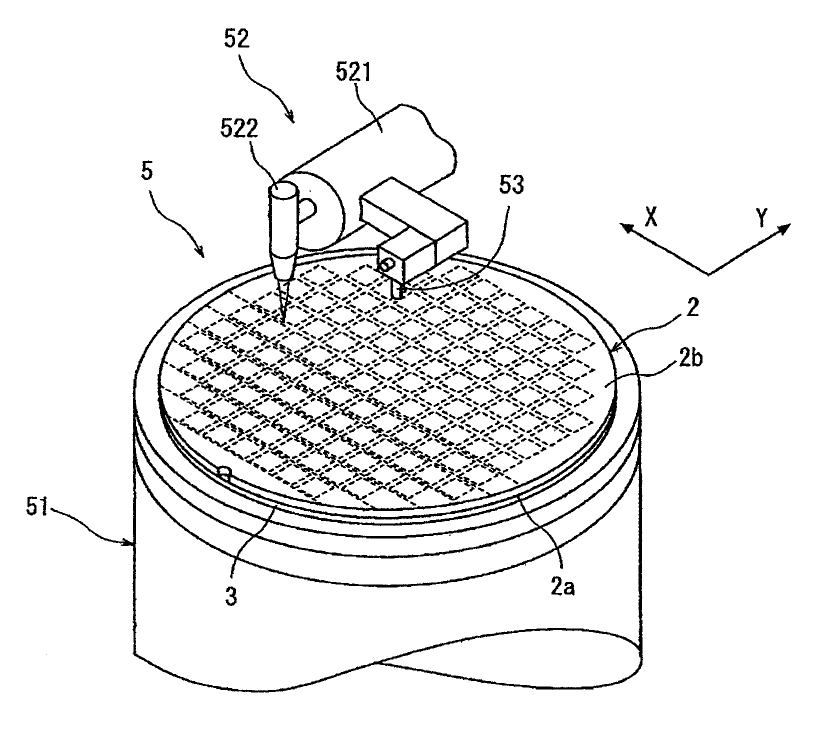
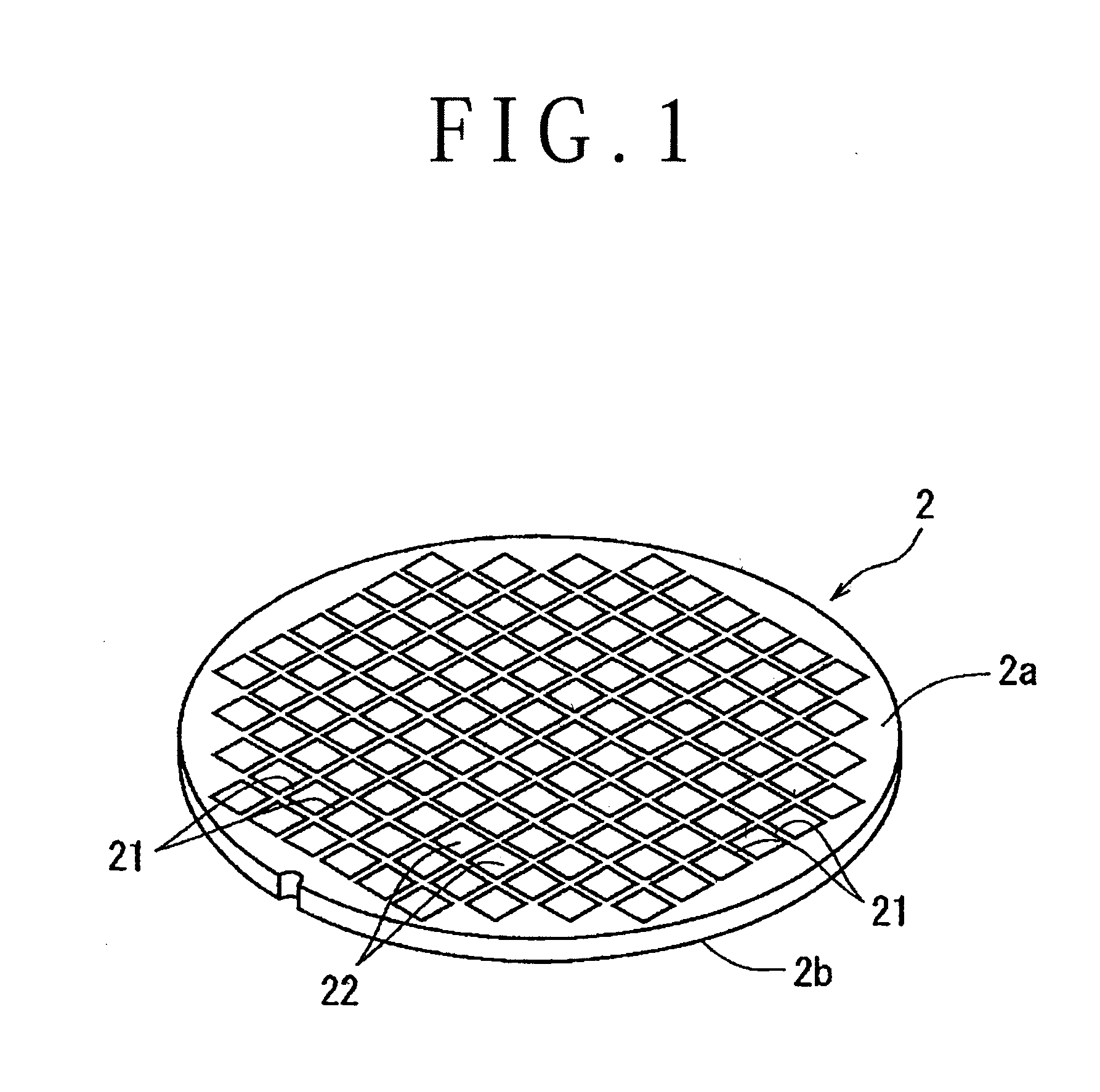
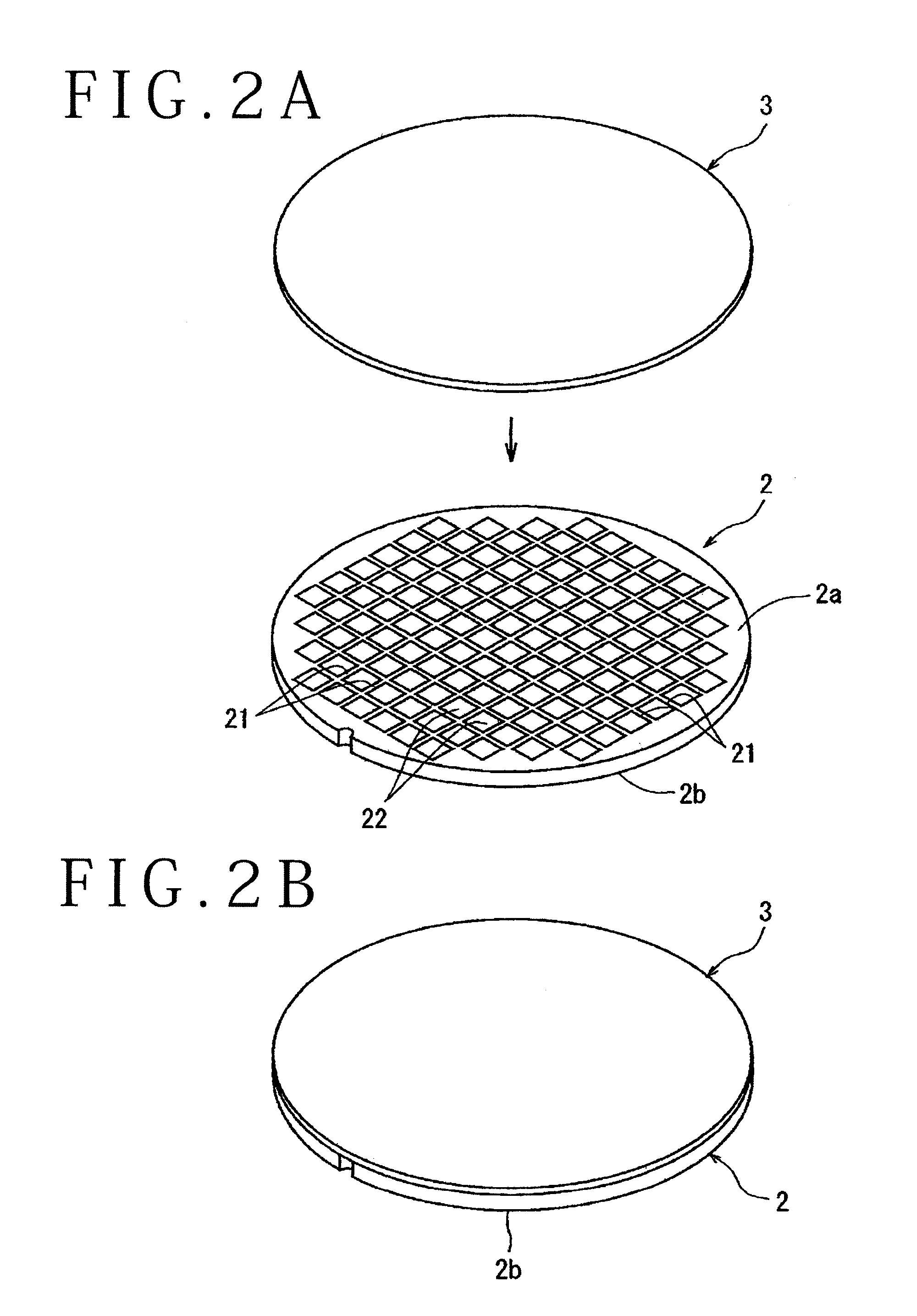
[0030]A preferred embodiment of a wafer processing method according to the present invention will now be described in detail with reference to the attached drawings. FIG. 1 is a perspective view of a semiconductor wafer 2 as a wafer to be processed by the method of the present invention. The semiconductor wafer 2 shown in FIG. 1 is formed from a silicon wafer having a thickness of 600 μm, for example. A plurality of crossing streets 21 are formed on a front side 2a of the semiconductor wafer 2 to thereby partition into a plurality of rectangular regions where a plurality of devices 22 such as ICs and LSIs are respectively formed. There will now be described the wafer processing method of dividing the semiconductor wafer 2 along the streets 21 to obtain the individual devices 22.

[0031]First, a protective member attaching step is performed in such a manner that a protective member is attached to the front side 2a of the semiconductor wafer 2 to protect the devices 22 formed on the fro...


PUM


Abstract

A wafer processing method of dividing a wafer along streets. The wafer processing method includes a protective tape attaching step of attaching a protective tape to the front side of the wafer, a modified layer forming step of holding the wafer through the protective tape on a chuck table of a laser processing apparatus under suction and next applying a laser beam having a transmission wavelength to the wafer from the back side of the wafer along the streets, thereby forming a modified layer inside the wafer along each street, and a wafer dividing step of canceling suction holding of the wafer by the chuck table and next applying an air pressure to the wafer now placed on the holding surface in the condition where horizontal movement of the wafer is limited, thereby dividing the wafer along each street where the modified layer is formed, thus obtaining individual devices.

Description

BACKGROUND OF THE INVENTION[0001]1. Field of the Invention[0002]The present invention relates to a wafer processing method of dividing a wafer along a plurality of crossing streets formed on the front side of the wafer to thereby partition a plurality of regions where a plurality of devices are respectively formed along the streets, thus obtaining the individual devices.[0003]2. Description of the Related Art[0004]In a semiconductor device fabrication process, a plurality of crossing division lines called streets are formed on the front side of a substantially disk-shaped semiconductor wafer to thereby partition a plurality of regions where a plurality of devices such as ICs and LSIs are respectively formed. The semiconductor wafer is cut along the streets to thereby divide the regions where the devices are formed from each other, thus obtaining the individual devices. Further, an optical device wafer is provided by forming a gallium nitride compound semiconductor layer or the like ...

Claims


Application Information

Patent Timeline
Patent Type & Authority Applications(United States)
IPC IPC(8): H01L21/78
CPCH01L21/78B24B7/228H01L21/683H01L21/67092H01L21/30
Inventor KOBAYASHI, SATOSHIZHAO, JINYAN
Owner DISCO CORP
Why Eureka
Try Eureka