Substrate processing system, transfer module, substrate processing method, and method for manufacturing semiconductor element

a technology of substrate processing and transfer module, which is applied in the direction of thin material processing, electrical equipment, article separation, etc., can solve the problems of inability to improve throughput (number of substrates processed per unit time), the substrate cannot be continuously processed under vacuum condition, and the substrate processing system cannot achieve the effect of reducing the footprin

Active Publication Date: 2013-08-08
TOKYO ELECTRON LTD
View PDF21 Cites 221 Cited by
  • Summary
  • Abstract
  • Description
  • Claims
  • Application Information

AI Technical Summary

Benefits of technology

[0020]The present invention provides a substrate processing system which is capable of provid

Problems solved by technology

However, the substrate processing system has a drawback in that the substrate cannot be continuously processed under vacuum condition when the substrate has to be moved between the processing chambers 1 because the substrate needs to pass through the atmosphere of the loader module 3 before it is passed over from one processing chamber 1 to another.
However, since one vacuum transfer robot 9 h

Method used


Image

  • Substrate processing system, transfer module, substrate processing method, and method for manufacturing semiconductor element
  • Substrate processing system, transfer module, substrate processing method, and method for manufacturing semiconductor element
  • Substrate processing system, transfer module, substrate processing method, and method for manufacturing semiconductor element

Examples


embodiment 1

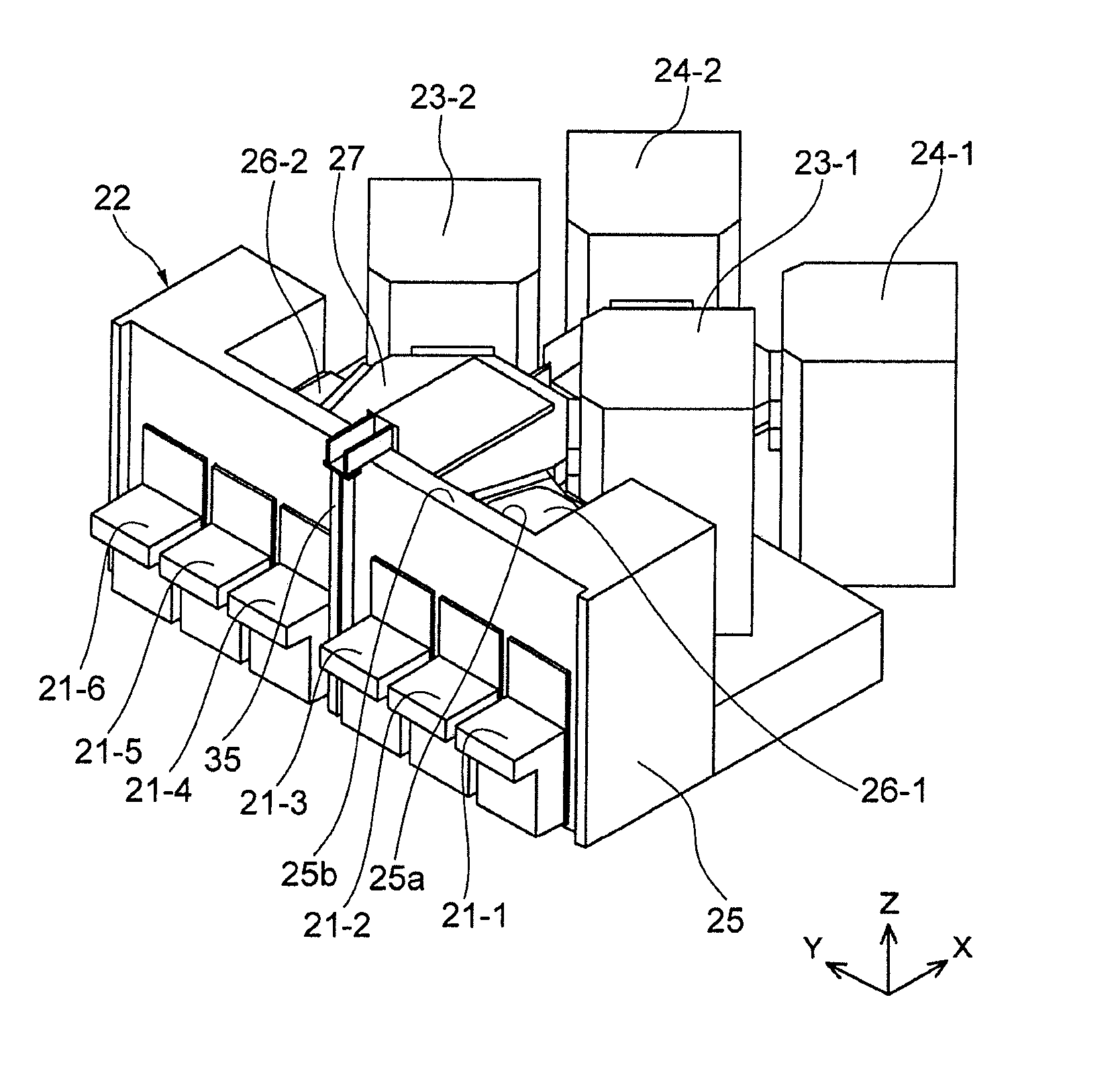
[0089]FIG. 3 shows a configuration (mainly, a front side system configuration) of a substrate processing system in accordance with a first embodiment of the present invention. The substrate processing system includes an elongated rectangular parallelepiped loader module 22 provided with a plurality of (e.g., six) ports 21-1 to 21-6 on which a plurality of cassettes (not shown) is arranged in a horizontal direction, and a plurality of (e.g., four) processing chambers 23-1, 23-2, 24-1 and 24-2.

[0090]The loader module 22 includes a rectangular parallelepiped atmospheric transfer chamber 25 extending in one direction (Y direction). The plurality of ports 21-1 to 21-6 is traversely arranged in a line at one side of the atmospheric transfer chamber 25. In a plan view, the atmospheric transfer chamber 25 is extended in the arrangement direction (Y direction) of the plurality of ports 21-1 to 21-6. A cassette in which a plurality of unprocessed substrates W is accommodated is loaded or set ...

embodiment 2

[0177]FIG. 24 shows a substrate processing system in accordance with a second embodiment of the present invention. In this embodiment, the second transfer chamber 30 is connected to the first transfer chamber 27 via a connection chamber 96, instead of being connected to the loader module 22 via the second load-lock chambers 29-1 and 29-2. Since the first transfer chamber 27 and the second transfer chamber 30 have different heights, the connection chamber 96 is provided with an elevation mechanism (an elevator) for elevating a substrate W.

[0178]The loader module 22, the first load-lock chambers 26-1 and 26-2, the first transfer chamber 27, the first processing chambers 23-1 and 23-2 and the second processing chambers 24-1 and 24-2 have the same configurations as those in the substrate processing system in accordance with the first embodiment and therefore, explanation thereof will be omitted while using the same reference numerals.

[0179]Since the first transfer chamber 27 and the sec...

embodiment 3

[0187]FIG. 26 is a plan view of a substrate processing system in accordance with a third embodiment of the invention. A substrate processing system of the present embodiment is different from the substrate processing system of the first embodiment in that the first load-lock chambers 26-1 and 26-2 and the first transfer chamber 27 of the first transfer unit 28 are not vertically overlapped with the loader module 22. The basic configurations of the first and second transfer units 28 and 31, e.g., the first transfer unit 28 including the first load-lock chambers 26-1 and 26-2 and the first transfer chamber 27, the second transfer unit 31 including the second load-lock chambers 29-1 and 29-2 and the second transfer chamber 30, and a portion of the first transfer unit 28 making vertical overlap with a portion of the second transfer unit 31, are the same as those in the substrate processing system of the first embodiment and therefore, explanation thereof will be omitted while using the ...


PUM


Abstract

A substrate processing system is provided with: a first transfer unit, which extends from a loader module to a first processing chamber for processing substrates, to transfer the substrates; and a second transfer unit, which is provided below or above the first transfer unit and extends from the loader module to a second processing chamber for processing substrates, to transfer the substrates. The first processing chamber and the second processing chamber do not overlap in the vertical direction, and are disposed at positions separated from each other in a plan view. At the same time, at least a part of the first transfer unit and at least a part of the second transfer unit overlap each other in the vertical direction.

Description

FIELD OF THE INVENTION[0001]The present invention relates to a substrate processing system and a substrate transfer module which transfers a substrate such as a semiconductor substrate, a liquid crystal substrate, an organic EL element and the like into a plurality of processing chambers.BACKGROUND OF THE INVENTION[0002]In a manufacturing process of a semiconductor device, a FPD (flat panel display), an organic EL (Electro Luminescence) element, a solar cell and the like, a semiconductor substrate, a glass substrate or the like is subjected to various processes such as film forming, etching, ashing, oxidation, nitriding, doping, diffusion and the like. These processes are performed in depressurized processing chambers if plasma is used.[0003]A multi-chamber type substrate processing system for performing simultaneous substrate processing in a plurality of processing chambers is commonly used to improve a throughput. FIG. 1 shows a substrate processing system as an example of convent...

Claims


Application Information

Patent Timeline
IPC IPC(8): H01L21/677
CPCH01L21/67161H01L21/67178H01L21/67184H01L21/67739H01L21/67196H01L21/67201H01L21/67703H01L21/6719H01L21/67742H01L21/67167
Inventor HIROKI, TSUTOMU
Owner TOKYO ELECTRON LTD
Why Eureka
Try Eureka