Semiconductor process

Active Publication Date: 2013-08-08
UNITED MICROELECTRONICS CORP
View PDF1 Cites 14 Cited by
  • Summary
  • Abstract
  • Description
  • Claims
  • Application Information

AI Technical Summary

Benefits of technology

The invention provides a semiconductor process that uses ozone saturated deionized water to create an oxide layer on a substrate, followed by the addition of a dielectric layer and annealing to reduce effective oxide thickness and gate leakage. The technique results in a thinner layer and improved performance of the semiconductor structure.

Problems solved by technology

With the trend towards scaling down the size of semiconductor devices, conventional poly-silicon gates face such problems as lower performances due to boron penetration and unavoidable depletion effect, which enlarges the equivalent thickness of the gate dielectric layer, reduces the gate capacitance, and worsens the driving force of the devices.
AS the size of semiconductor components are miniaturized, the effective oxide thickness (EOT) and the gate leakage (Jg) are difficult to minimize because of process limitations.

Method used


Image

  • Semiconductor process
  • Semiconductor process
  • Semiconductor process

Examples


Embodiment Construction

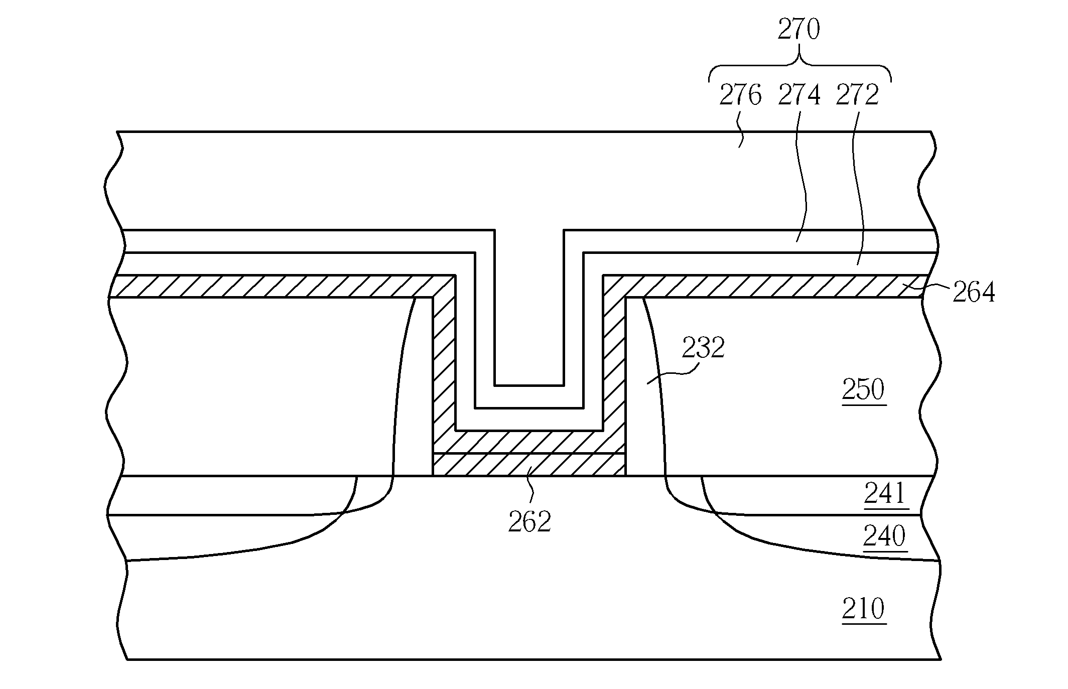
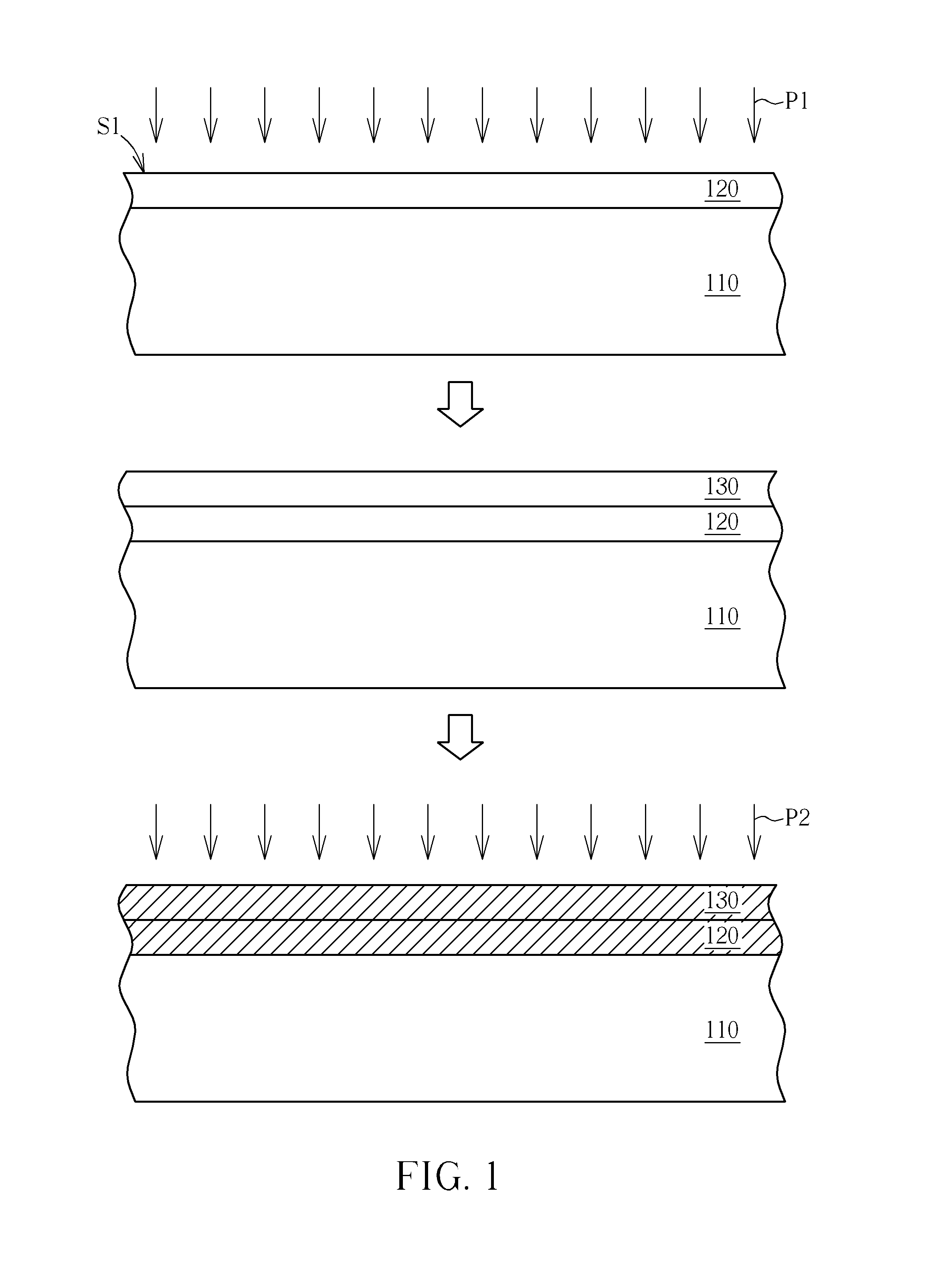
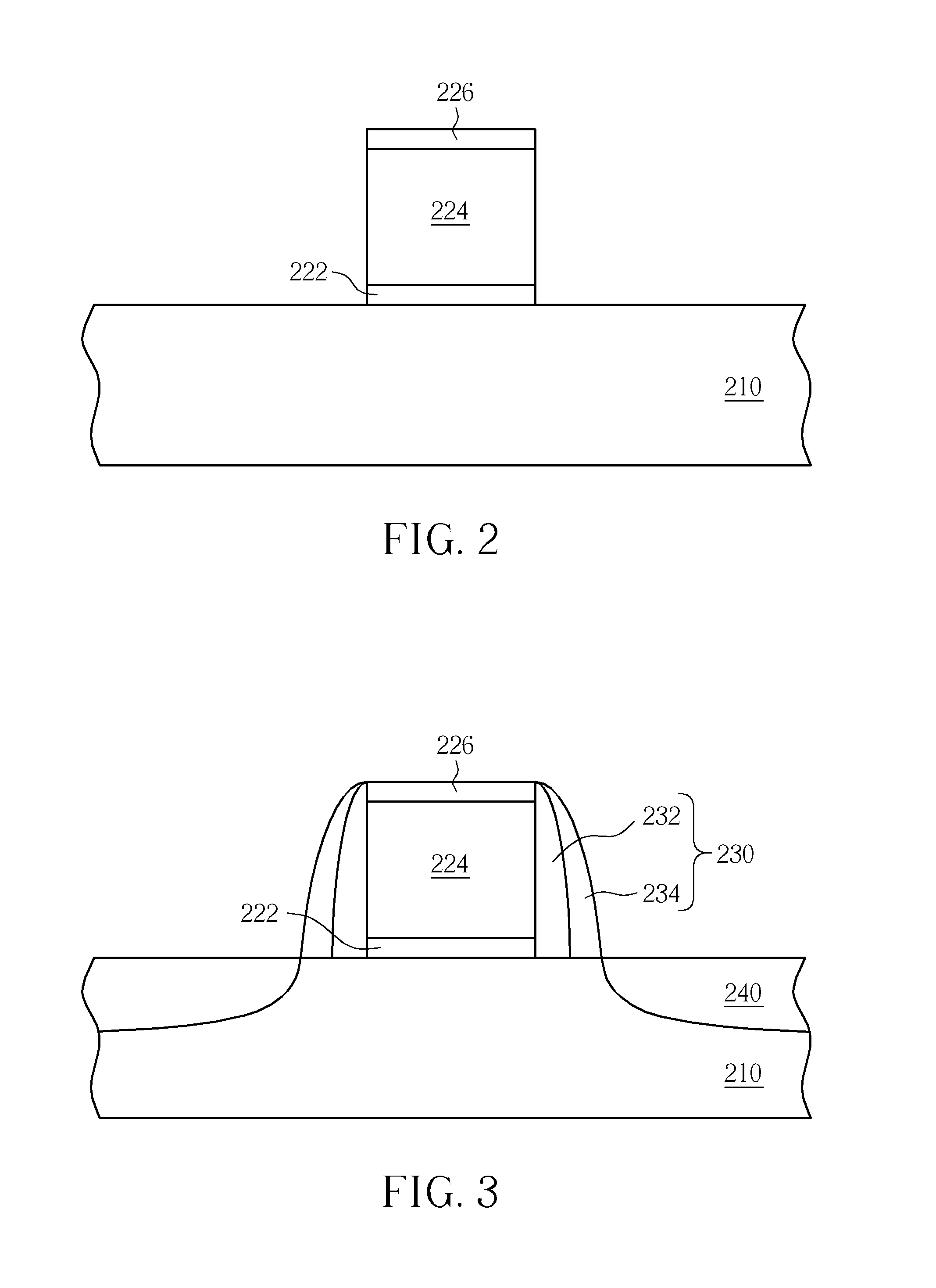
[0014]FIG. 1 schematically depicts a cross-sectional view of a semiconductor process according to one embodiment of the present invention. As shown in the top part of FIG. 1, a substrate 110 is provided. The substrate 110 may be a semiconductor substrate such as a silicon substrate, a silicon containing substrate, a III-V group-on-silicon (such as GaN-on-silicon) substrate, a graphene-on-silicon substrate or a silicon-on-insulator (SOI) substrate. A pre-treatment process (not shown) may be selectively performed to clean impurities such as native oxides on the substrate 110. The pre-treatment process (not shown) may be a dilute hydrofluoric acid containing (DHF) pre-treatment process, but it is not limited thereto. An ozone saturated deionized water process P1 is performed to form an oxide layer 120 on the substrate 110. In the present invention, an oxide layer 120 can be formed on the substrate 110 by performing an ozone saturated deionized water process P1. However, an oxide layer ...


PUM


Abstract

A semiconductor process includes the following steps. A substrate is provided. An ozone saturated deionized water process is performed to form an oxide layer on the substrate. A dielectric layer is formed on the oxide layer. A post dielectric annealing (PDA) process is performed on the dielectric layer and the oxide layer.

Description

BACKGROUND OF THE INVENTION[0001]1. Field of the Invention[0002]The present invention relates generally to a semiconductor process, and more specifically to a semiconductor process, wherein an ozone saturated deionized water process is carried out to form an oxide layer and an annealing process is performed after a dielectric layer is formed.[0003]2. Description of the Prior Art[0004]Poly-silicon is conventionally used as a gate electrode in semiconductor devices such as metal-oxide-semiconductors (MOS). With the trend towards scaling down the size of semiconductor devices, conventional poly-silicon gates face such problems as lower performances due to boron penetration and unavoidable depletion effect, which enlarges the equivalent thickness of the gate dielectric layer, reduces the gate capacitance, and worsens the driving force of the devices. Therefore, work function metals that are suitable for use as the high-K gate dielectric layer are used to replace the conventional poly-si...

Claims


Application Information

Patent Timeline
IPC IPC(8): H01L21/336
CPCH01L29/66477H01L21/28185H01L29/7833H01L29/513H01L29/66545H01L29/51
Inventor CHEN, YING-TSUNGLIN, CHIEN-TINGFU, SSU-ITSAI, SHIH-HUNGCHIANG, WEN-TAICHEN, CHIH-WEIYEH, CHIU-HSIENWANG, SHAO-WEIWANG, KAI-PING
Owner UNITED MICROELECTRONICS CORP
Why Eureka
Try Eureka