InGaN-Based Double Heterostructure Field Effect Transistor and Method of Forming the Same

Inactive Publication Date: 2013-08-15
IQE KC
View PDF2 Cites 12 Cited by
  • Summary
  • Abstract
  • Description
  • Claims
  • Application Information

AI Technical Summary

Benefits of technology

[0009]The present invention provides high-performance InGaN-based DHFETs with improved 2DEG mobility and reduced leakage current. A DHFET constructed in accordance with the present invention comprises a substrate, a GaN back-barrier buffer layer formed on the substrate, and having a nucleation layer between the substrate and the GaN, a narrow band-gap channel consisting of a Ga1-xInxN ternary alloy (0.04≦x≦1) or, alternatively, an InGaN/GaN superlattice (SL) formed on the GaN back-barrier buffer layer opposite to the substrate, a GaN spacer layer formed on said narrow band-gap channel layer opposite to the GaN back-barrier buffer layer and a carrier supplying barrier layer consisting of an Al1-yInyN (0.14<x≦0.20) ternary alloy formed on said GaN spacer layer opposite to the narrow band-gap channel. The GaN spacer layer and the narrow ban

Problems solved by technology

While GaN-based field effect transistors (FET) are very promising both in terms of underlying material properties and demonstrated device results, fundamental physical limitations exist when scaling conventional GaN devices to deep submicron dimensions necessary to realize their potential for ultra-high power and ultra-high frequency operation.
However, these devices still lack control of the channel thickness because the 2DEG is formed in GaN, the same material as the buffer layer, and therefore suffer from short-channel effects (D. S. Lee, X. Gao, S. Guo, D. Kopp, P

Method used


Image

  • InGaN-Based Double Heterostructure Field Effect Transistor and Method of Forming the Same
  • InGaN-Based Double Heterostructure Field Effect Transistor and Method of Forming the Same
  • InGaN-Based Double Heterostructure Field Effect Transistor and Method of Forming the Same

Examples


Embodiment Construction

[0019]A description of example embodiments of the invention follows.

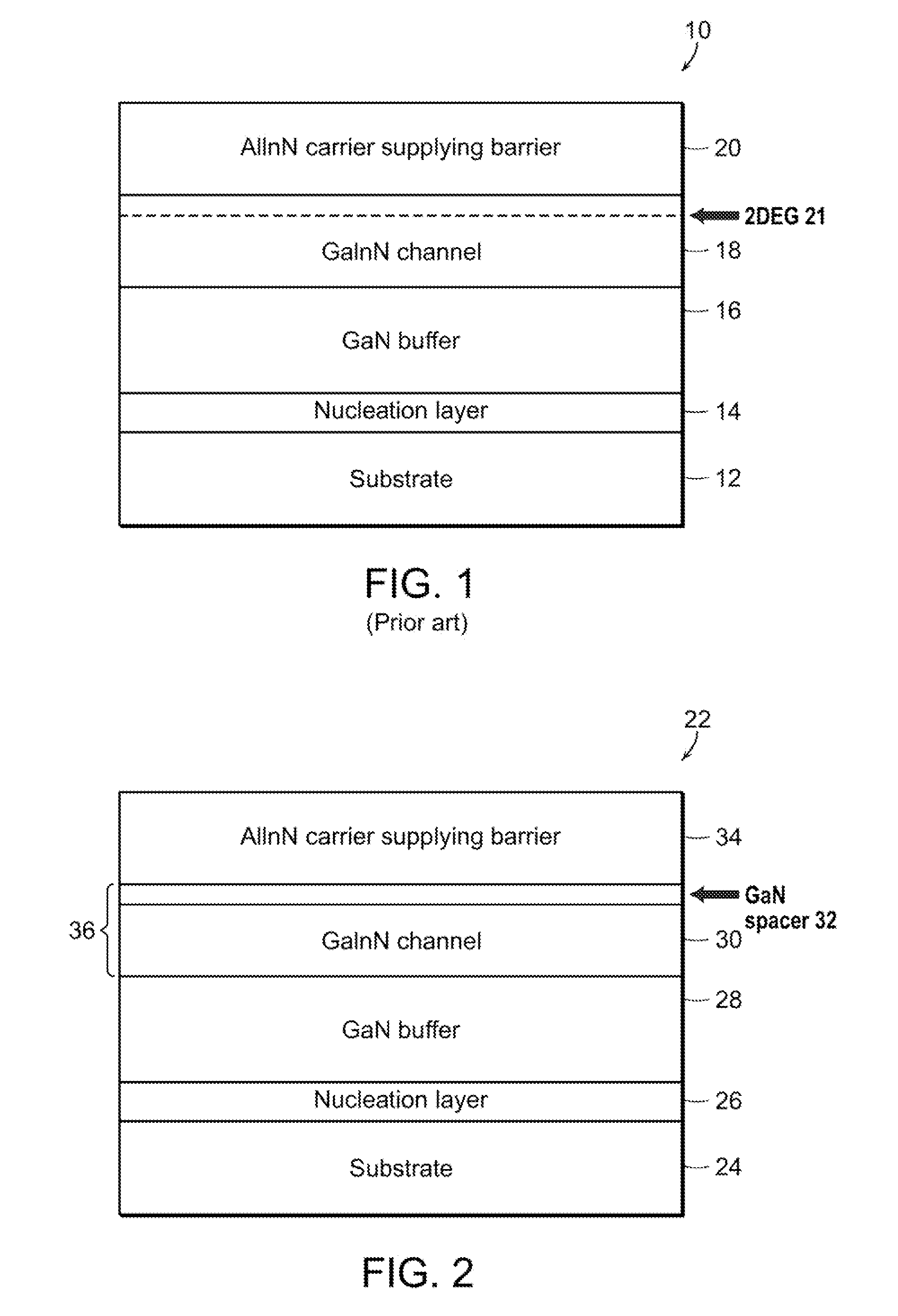
[0020]FIG. 1 illustrates a prior art InGaN-based DHFET structure 10 that comprises a substrate 12, a nucleation layer 14 adjacent to the substrate, a GaN back-barrier buffer layer 16 adjacent to the nucleation layer 14 opposite the substrate 12, a InxGa1-xN (0.0418 adjacent to the GaN buffer layer 16, opposite the substrate 12, and an Al1-yInyN (0.1420 adjacent to the InxGa1-xN 18, opposite the GaN back-barrier buffer layer 16. A 2DEG region 21 is at the interface between InxGa1-xN channel layer 18 and Al1-yInyN carrier-supplying layer 20.

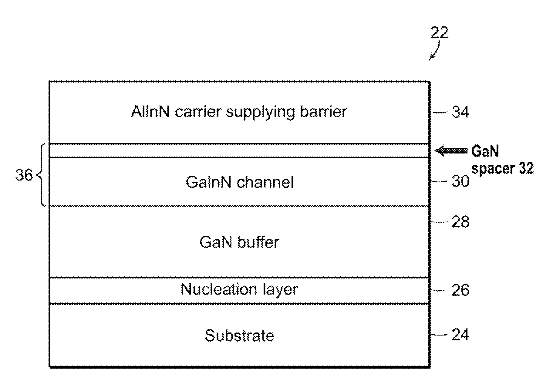
[0021]FIG. 2 shows one embodiment of the InGaN-based DHFET 22 constructed in accordance with the present invention. It comprises a substrate 24, a nucleation layer 26 adjacent to the substrate 24, a GaN back-barrier buffer layer 28 adjacent to the nucleation layer 26, opposite the substrate 24, a InxGa1-xN channel layer 30 adjacent to the GaN back-barrier buffer layer 28, opposite ...


PUM


Abstract

A double heterojunction field effect transistor (DHFET) includes a substrate, a buffer layer consisting of GaN back-barrier buffer layer formed on the substrate, a channel layer consisting of an InxGa1-xN ternary alloy in one embodiment, and in another embodiment, InGaN/GaN superlattice (SL) formed on the GaN back-barrier buffer layer opposite to the substrate. A GaN spacer layer is formed on the InxGa1-xN or InGaN/GaN superlattice channel layer opposite to the GaN buffer layer and a carrier-supplying layer consisting of an Al1-yInyN ternary alloy is formed on the GaN spacer layer opposite to the channel layer. A preferred thickness of the GaN spacer layer is less than about 1.5 nm. The InGaN/GaN SL preferably includes 1 to 5 InGaN—GaN pairs and a preferred thickness of the InGaN layer in the InGaN/GaN SL is equal to or less than about 0.5 nm. A two-dimensional electron gas is formed at the interface between the InxGa1-xN or InGaN/GaN SL channel and GaN spacer layers.

Description

RELATED APPLICATIONS[0001]This application claims the benefit of U.S. Provisional Application No. 61 / 588,014, filed Jan. 18, 2012, the relevant teachings of which are incorporated herein by reference in their entirety.BACKGROUND OF THE INVENTION[0002]The present invention relates to double heterojunction field effect transistors that incorporate nitride based active layers and contain a high mobility two-dimentional electron gas.[0003]While GaN-based field effect transistors (FET) are very promising both in terms of underlying material properties and demonstrated device results, fundamental physical limitations exist when scaling conventional GaN devices to deep submicron dimensions necessary to realize their potential for ultra-high power and ultra-high frequency operation. Two dimensions of the nitride transistor structure are particularly essential.[0004]These are the barrier and channel thicknesses which have to be minimized to achieve high performance. For a conventional AlGaN / ...

Claims


Application Information

Patent Timeline
IPC IPC(8): H01L29/15H01L21/02H01L29/205
CPCH01L29/7783H01L29/155H01L29/151H01L29/205H01L21/02507H01L29/2003
Inventor LABOUTIN, OLEGCAO, YUJOHNSON, WAYNE
Owner IQE KC
Why Eureka
Try Eureka