This helps you quickly interpret patents by identifying the three key elements:
Problems solved by technology
Method used
Benefits of technology
Benefits of technology
This patent presents a method for producing a large area of graphene and transferring it to a different substrate, which overcomes the limitations of previous methods. The method includes growing a graphene layer on a metal layer on a donor substrate, laminating a dry film photo-resist onto the graphene layer, and then chemically etching the metal layer to create an initial structure. This structure is then transferred to the final substrate and the dry film photo-resist is removed to create a final structure with a transferred graphene layer. The method allows for the use of a temporary substrate, which can be rigid or flexible, and can accommodate different sizes and shapes of final substrates. Additionally, the method allows for the use of a thermal releasing tape to better mechanically support the dry film photo-resist during the transfer process. The final structure produced using the method has a transferred graphene layer with good functional and structural characteristics.
Problems solved by technology
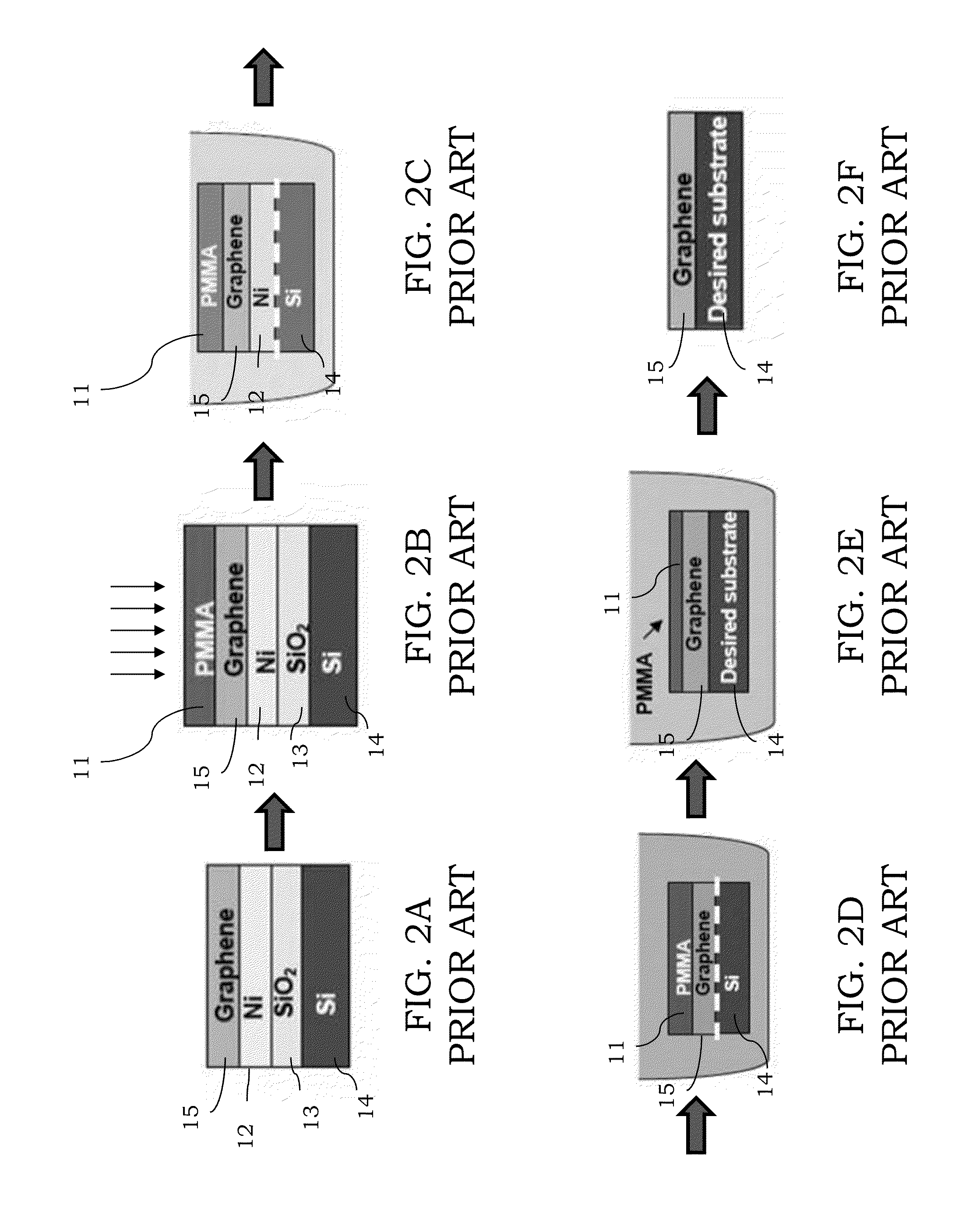
Nevertheless, even if this method is very simple and low cost, it cannot be used for industrial production, due to the reduced dimensions of the graphene sheets so produced.
In addition, the produced graphene has many defects due to the siliconcarbide superficial morphology.
Even if a large number of graphene monolayer films are so produced, the total weight being up to 50%, the solvents which have to be used are too expensive and dangerous.
Even if all the above described chemical techniques are advantageous for the scalability and flexibility, they do not guarantee a control of the number of dispersed graphitelayers.
Even if this technique is advantageous under many aspects, such as high productivity and scalability on a large area, it has the drawback that the glue on the tape is randomically kept on the transferred graphene layer, causing breaks on it.
This technique has the drawback that it is not scalable on a large area and it is not used for mass production.
This technique has the drawback that the graphene productivity is very limited and involves a transferring on very small areas.
Method used
Image
Click on the blue label to locate the original text in one second.
Reading with bidirectional positioning of images and text.
Examples
second embodiment
[0081]With reference to such figures, and in particular to FIGS. 3A-3G and, respectively, to FIGS. 4A-4G, different steps of a first and, respectively, a method for transferring graphene from a donor substrate to a different or final substrate are shown.
[0082]It should be noted that the process steps being described hereinafter do not deal with a complete manufacturing process of a wafer. The present disclosure can be carried out along with the manufacturing techniques of integrated circuits being usually employed in the field.
[0083]Moreover, figures showing schematic views of the integrated structure during the manufacturing are not drawn in scale, being on the contrary drafted so as to emphasize features of the disclosure.
[0084]In particular, the method for transferring graphene from a donor substrate to a different or final substrate comprises, both in the first and in the second embodiments, steps shown respectively in FIGS. 3A-3E and 4A-4E
[0085]Both method embodiments provide a...
first embodiment
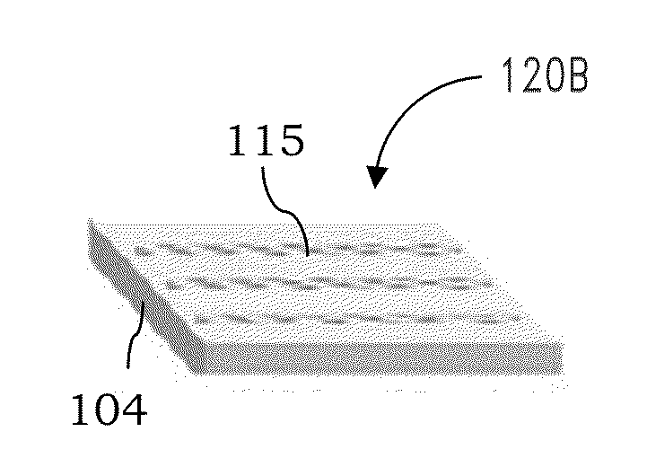
[0091]Moreover, the method further comprises:[0092]removing the dry film photo-resist 106; and[0093]obtaining a final structure 120A comprising the final substrate 104 with the transferred graphene layer 105.
[0094]It should be remarked that the transferred graphene layer 105 is a monolayer. Moreover, it should be noted that a dry film negative photo-resist could be usefully used.
[0095]In particular, according to the first embodiment, the method further comprises, after the step of thermally releasing the tape 101:[0096]chemically etching away the entire dry film photo-resist 106, as shown in FIG. 3F, thereby obtaining the final structure 120A comprising the final substrate 104 with the transferred graphene layer 105, as shown in FIG. 3G.
[0097]According to the second embodiment, the method further comprises, after the step of thermally releasing the tape 101, the steps of:[0098]exposing the dry film photo-resist 106 to UV light using a lithographic mask 125, in particular a dry film...
PUM
Abstract
A method transfers a graphene layer from a donor substrate onto a final substrate. The method includes: providing a metal layer on the donor substrate; and growing a graphene layer on the metal layer. The method also includes: laminating a dry film photo-resist on the graphene layer; laminating a tape on the dry film photo-resist; chemically. etching the metal layer, obtaining an initial structure that includes the tape, the dry film photo-resist and the graphene layer; laminating the initial structure on the final substrate; thermally realizing the tape, so as to obtain an intermediate structure that includes the dry film photo-resist, the graphene layer and the final substrate; removing the dry film photo-resist; and obtaining a final structure that includes the final substrate with a transferred graphene layer.
Description
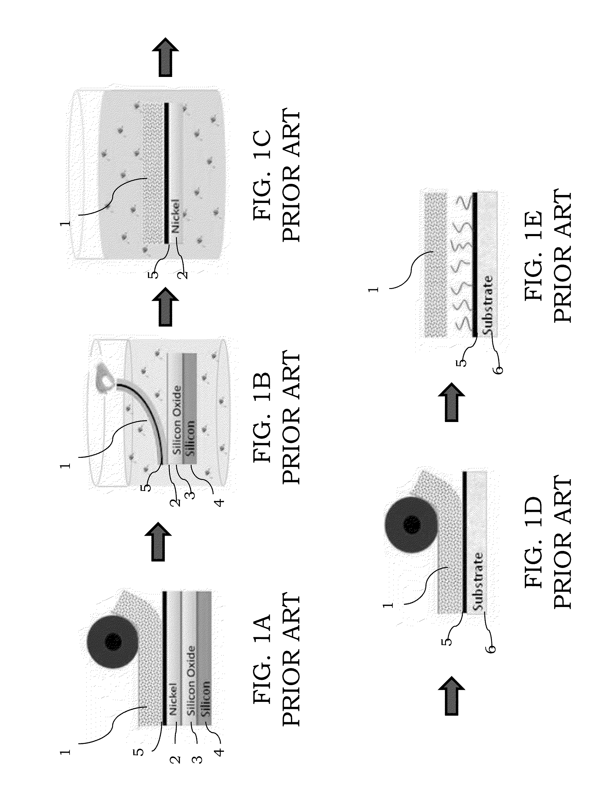
BACKGROUND[0001]1. Technical Field[0002]The present disclosure relates to a method for transferring a graphene layer onto a substrate.[0003]The disclosure refers, in particular, but not exclusively, to a method for transferring a graphene layer from a donor substrate to a different substrate, of the type comprising a rigid or a flexible material, and the following description is made with reference to this field of application just for explanation convenience.[0004]2. Description of the Related Art[0005]In recent years, many studies have been done on the production and transferring of graphene, which is a material comprising a single layer of carbon atoms placed in an hexagonal crystal lattice and having excellent electrical and optical properties. It is well known, in fact, that graphene is a zero gap semiconductor material having high charges mobility (10,000 cm2 / Vs), high conductivity, high transmittance (˜98%) and excellent mechanical properties (high tensile stress equal to 130...
Claims
Application Information
Patent Timeline
Application Date:The date an application was filed.
Publication Date:The date a patent or application was officially published.
First Publication Date:The earliest publication date of a patent with the same application number.
Issue Date:Publication date of the patent grant document.
PCT Entry Date:The Entry date of PCT National Phase.
Estimated Expiry Date:The statutory expiry date of a patent right according to the Patent Law, and it is the longest term of protection that the patent right can achieve without the termination of the patent right due to other reasons(Term extension factor has been taken into account ).
Invalid Date:Actual expiry date is based on effective date or publication date of legal transaction data of invalid patent.

