

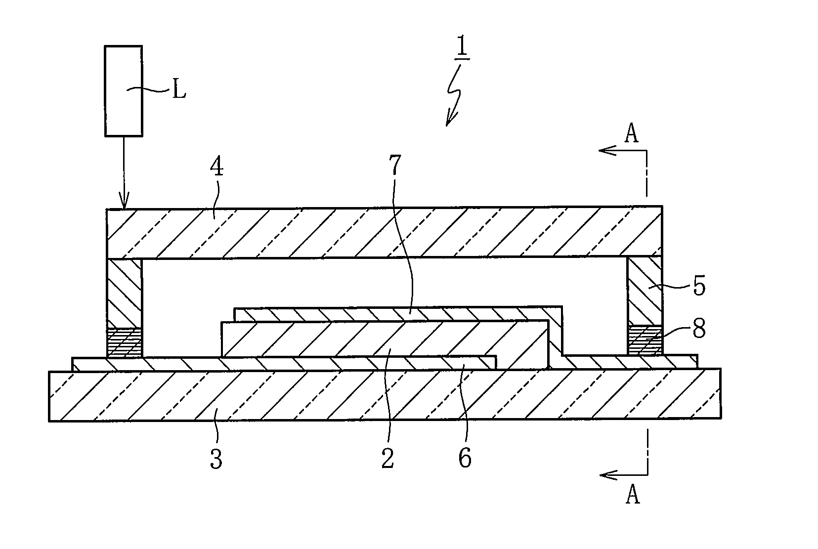
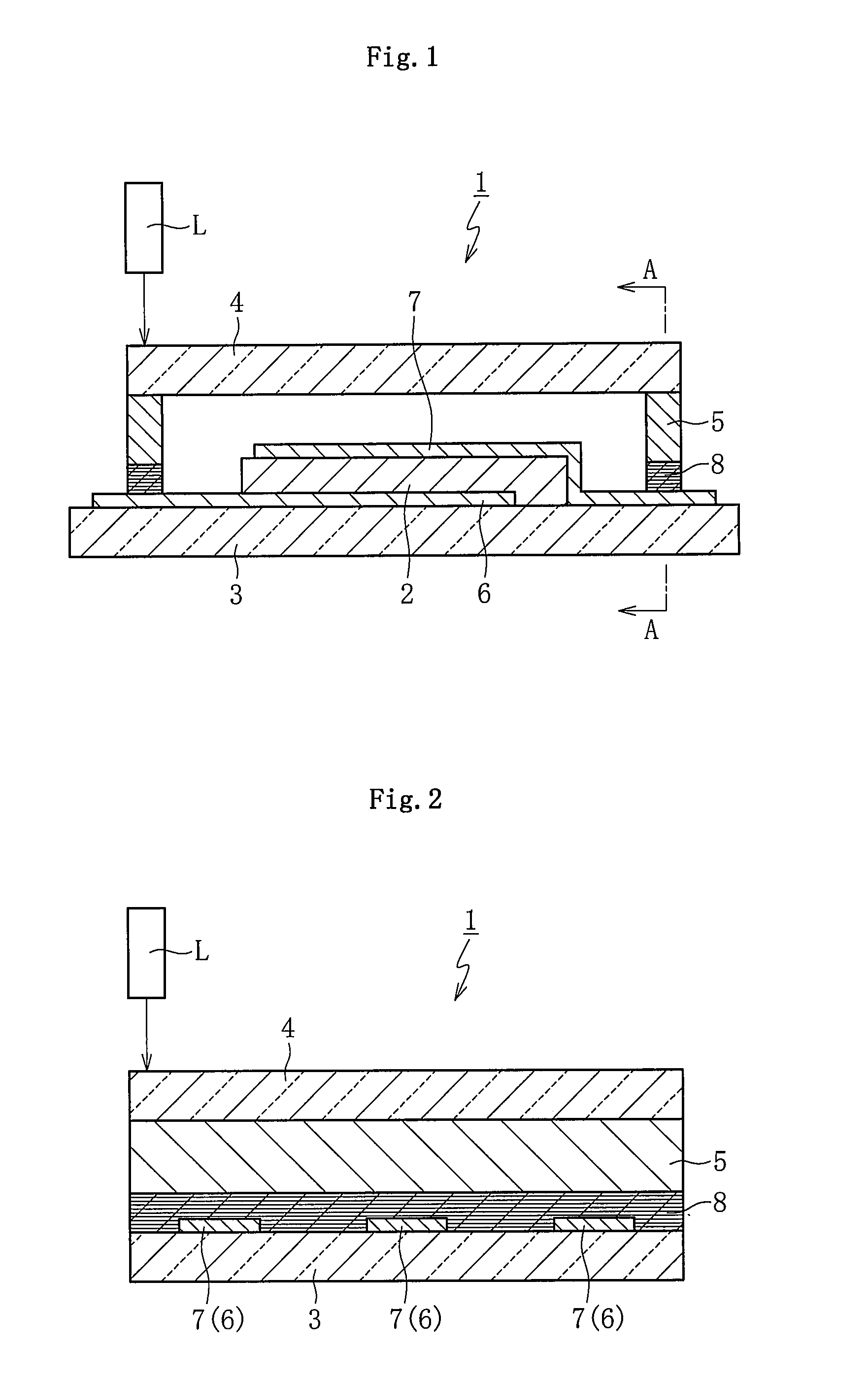
Electrical element package
- Summary
- Abstract
- Description
- Claims
- Application Information
AI Technical Summary
Benefits of technology
Problems solved by technology
Method used
Image

Examples
example 1
[0131]First, the first aspect of the present invention is described in detail based on examples. It should be noted that the first aspect of the present invention is not limited to the following examples. The following examples are mere exemplifications.
[0132](Simulation of Frequency Characteristic of Reflectance)
[0133]Design values of film configurations of examples (No. 2 to No. 4) of the multilayer dielectric film used for the electrical element package according to the first aspect of the present invention are shown in Table 1. It should be noted that, in Table 1, a single-layer dielectric film is shown as a comparative example (No. 1).
TABLE 1No. 1No. 2No. 3No. 4No. 5First layerSi3N4Si3N4Si3N4Si3N4Si3N4(Thickness (nm))(100.6)(100.6)(100.6)(100.6)(100.6)Second layer—SiO2SiO2SiO2SiO2(Thickness (nm))(139.0)(139.0)(139.0)(139.0)Third layer—Si3N4Si3N4Si3N4Si3N4(Thickness (nm))(100.6)(100.6)(100.6)(100.6)Fourth layer——SiO2SiO2SiO2(Thickness (nm))(139.0)(139.0)(139.0)Fifth layer——Si3N4...
example 2
[0135](Measured Values of Frequency Characteristic of Reflectance)
[0136]Examples of film configurations of examples (No. 6 to No. 8) of the multilayer dielectric film used for the electrical element package according to the first aspect of the present invention are shown in Table 2.
TABLE 2No. 6No. 7No. 8First layerSi3N4Si3N4Si3N4(Thickness (nm))(100.6)(100.6)(100.6)Second layerSiO2SiO2SiO2(Thickness (nm))(139.0)(139.0)(139.0)Third layer—Si3N4Si3N4(Thickness (nm))(100.6)(100.6)Fourth layer—SiO2SiO2(Thickness (nm))(139.0)(139.0)Fifth layer—Si3N4Si3N4(Thickness (nm))(100.6)(100.6)Sixth layer—SiO2SiO2(Thickness (nm))(139.0)(139.0)Seventh layer——Si3N4(Thickness (nm))(100.6)Eighth layer——SiO2(Thickness (nm))(139.0)Total thickness239.6718.8958.4(nm)
[0137]Frequency characteristics of the reflectance of the examples (No. 6 to No. 8) are as shown in FIG. 6. Both the example with six layers (No. 7) and the example with eight layers (No. 8) had the maximum reflectance in the vicinity of the wav...
example 3
[0138](Temperature Measurement of Electrodes at the Time of Laser Welding)
[0139]The glass frit in a paste form was printed by screen printing at a thickness of 15 μm on the peripheral portion of the glass substrate with a dimension of 40 mm in length by 50 mm in width by 0.5 mm in thickness. Thereafter, preliminary firing was performed at 500° C. for one hour to temporarily cure the glass frit, thereby manufacturing the sealing substrate.
[0140]In this case, the glass frit containing 99 mass % of the inorganic powder and 1 mass % of the pigment was used. The inorganic powder contained in the glass frit comprises 60 vol % of SnO-based glass powder and 40 vol % of the refractory filler. The SnO-based glass powder contains, as a glass composition in terms of mol %, 59% of SnO, 20% of P2O5, 5% of ZnO, 15% of B2O3, and 1% of Al2O3. Further, the glass powder has an average particle diameter D50 of 2.5 μm and a maximum particle diameter Dmax of 7 μm. The refractory filler is made of zirconi...
PUM
| Property | Measurement | Unit |
|---|---|---|
| Fraction | aaaaa | aaaaa |
| Fraction | aaaaa | aaaaa |
| Percent by mass | aaaaa | aaaaa |
Abstract
Description
Claims
Application Information