Light emitting diode and fabrication method thereof

a technology of light-emitting diodes and fabrication methods, which is applied in the field of light-emitting diodes, can solve the problems of low light-emitting efficiency, unfavorable application, energy waste, etc., and achieve the effects of increasing the external quantum efficiency of leds, and increasing the light-emitting ra

Inactive Publication Date: 2013-08-22
XIAN SHENGUANG ANRUI PHOTOELECTRIC TECH
View PDF7 Cites 9 Cited by
  • Summary
  • Abstract
  • Description
  • Claims
  • Application Information

AI Technical Summary

Benefits of technology

[0007]One objective of the present invention is to provide a light emitting diode to solve the problem of low light extraction efficiency of conventional light emitting diodes.
[0008]Another objective of the present invention is to provide a fabrication method of light emitting diode with simple process to improve the light extraction efficiency of light emitting diodes.
[0023]With the adoption of the technical solution above, compared with the prior art, the present invention has the following advantages:
[0024]The sapphire substrate of the LED has a plurality of bifocal microlens structures on the surface close to the epitaxial layer. The bifocal microlens structures can increase the light reflected, raising the external quantum efficiency of the LED, thus increasing the light utilization rate of the LED. Furthermore, the formation of a plurality of bifocal microlens structures can improve the lattice matching between the sapphire substrate and other films, reducing the crystal defects in the film formed on the sapphire substrate, increasing the internal quantum efficiency of the LED, and making sure that the device is unlikely to break. In addition, the fabrication method of light emitting diode of the present invention has simple manufacturing process and is easy to implement.

Problems solved by technology

However, those semiconductor LEDs in the prior art have the problem of low light emitting efficiency.
For a conventional LED without packaging, the light extraction efficiency is generally several percent, because a large amount of energy gathers in the device and fails to give out, thus causing energy waste and also affecting the service life of the device.
However, the fabrication process of the LED requires the forming of a film structure stacked by multiple high refractive index layers and low refractive index layers on the substrate, which is a complicated technique and is unfavourable to put into application.
Therefore, how to provide a simple manufacturing process to increase the light reflected by the sapphire substrate and raise the external quantum efficiency of the LED has become a problem to be solved by those skilled in the art.

Method used


Image

  • Light emitting diode and fabrication method thereof
  • Light emitting diode and fabrication method thereof
  • Light emitting diode and fabrication method thereof

Examples


Embodiment Construction

[0030]To make the abovementioned purposes, features and merits of the present invention clearer and easier to understand, the present invention is further detailed by embodiments in combination with the drawings.

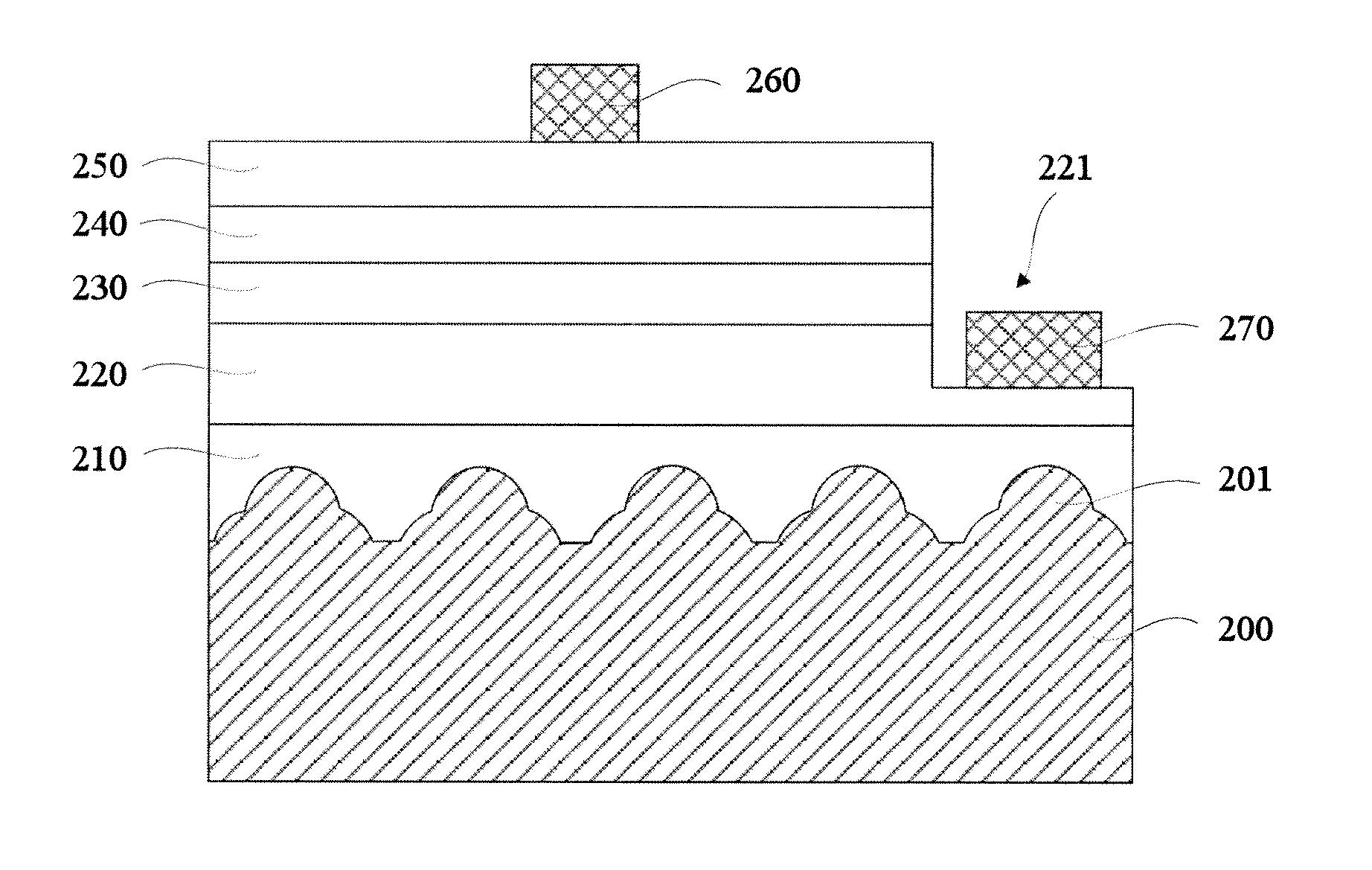
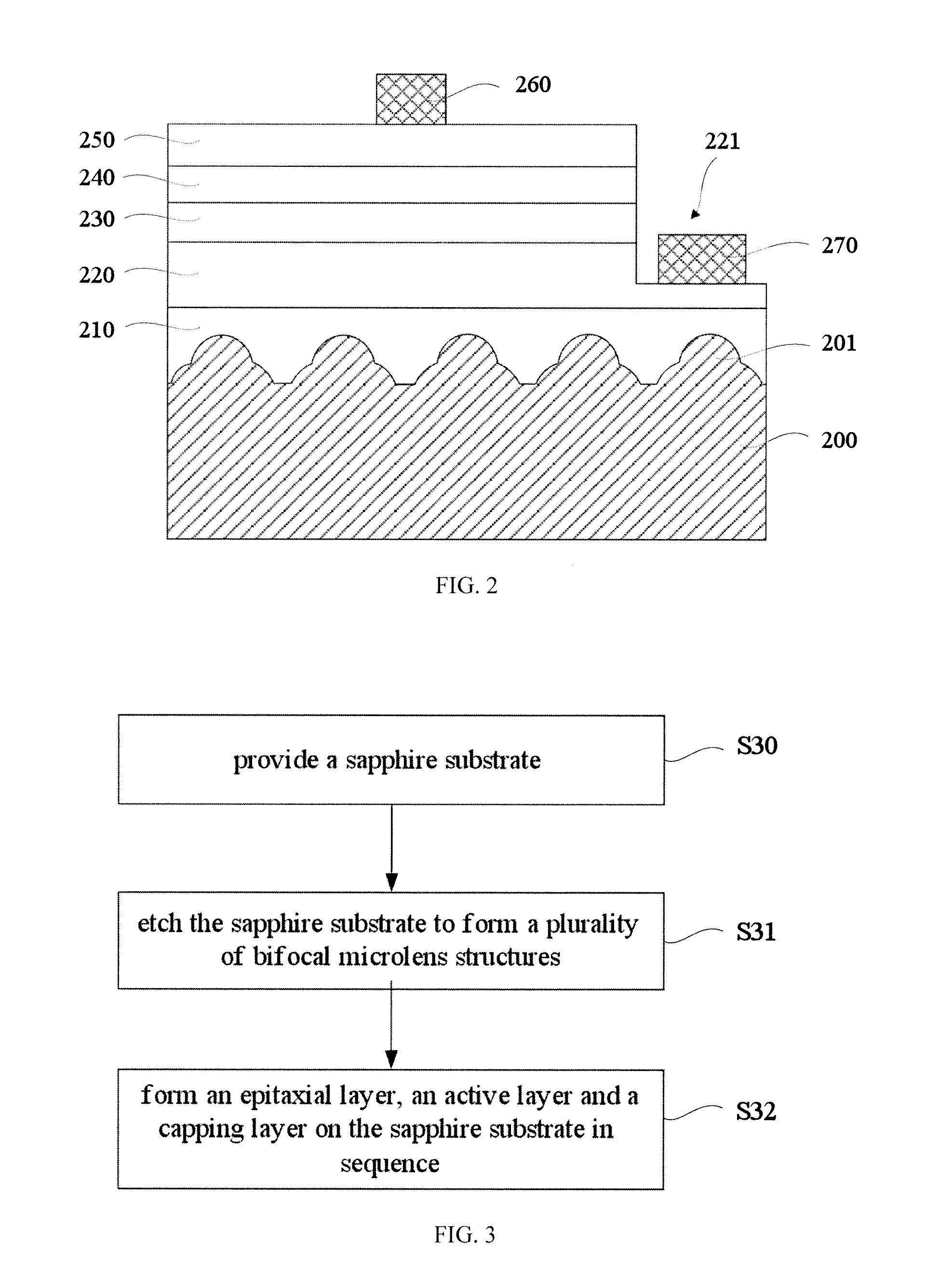
[0031]The core spirit of the present invention is to provide an LED and its fabrication method. The LED comprises: a sapphire substrate; an epitaxial layer, an active layer and a capping layer arranged on the sapphire substrate in sequence; wherein, a plurality of bifocal microlens structures are formed on the surface of the sapphire substrate close to the epitaxial layer. The bifocal microlens structures can increase the light reflected, raising the external quantum efficiency of the LED, thus increasing the light utilization rate of the LED. Furthermore, the formation of a plurality of bifocal microlens structures can improve the lattice matching between the sapphire substrate and other films, reducing the crystal defects in the film formed on the sapphire substrate, incre...


PUM


Abstract

An LED and its fabrication method are disclosed. The LED includes: a sapphire substrate (200); an epitaxial layer (220), an active layer (230) and a capping layer (240) arranged on the sapphire substrate (200) in sequence; wherein a plurality of bifocal microlens structures (201) are formed on the surface of the sapphire substrate (200) close to the epitaxial layer (220). The bifocal microlens structures (201) can increase the light reflected by the sapphire substrate (200), raising the external quantum efficiency of the LED, thus increasing the light utilization rate of the LED. Furthermore, the bifocal microlens structures (201) can improve the lattice matching between the sapphire substrate (200) and other films, reducing the crystal defects in the film formed on the sapphire substrate (200) and increasing the internal quantum efficiency of the LED.

Description

TECHNICAL FIELD[0001]The present invention relates to the light emitting field, and more particularly, to a light emitting diode and its fabrication method.BACKGROUND ART[0002]Light Emitting Diode (LED), having the advantages of long service life, low energy consumption and others, is widely used in various fields. In particular, with the greatly improved lighting performance, LED is often used as a light emitting device in lighting field. Wherein, the group III-V compound semiconductors such as gallium nitride (GaN), has tremendous application potential in high-brightness blue LED, blue laser and other photoelectric devices due to its wide band gap, high light emitting efficiency, high electronic saturation drift velocity, stable chemical property and other characteristics, which has aroused wide attention.[0003]However, those semiconductor LEDs in the prior art have the problem of low light emitting efficiency. For a conventional LED without packaging, the light extraction efficie...

Claims


Application Information

Patent Timeline
Patent Type & Authority Applications(United States)
IPC IPC(8): H01L33/04
CPCH01L21/0242H01L21/0243H01L21/02458H01L21/0254H01L33/04H01L33/007H01L33/20H01L33/02H01L21/02658
Inventor NIOU, CHORNGCHANG, ANDREW
Owner XIAN SHENGUANG ANRUI PHOTOELECTRIC TECH
Why Eureka
Try Eureka