GaN-Based LED electrode structure and manufacturing method thereof

A technology of electrode structure and manufacturing method, which is applied to circuits, electrical components, semiconductor devices, etc., can solve the problems of not mentioning the method of forming the coated electrode, the adhesion is not ideal, and the cost of the electrode structure is high, so as to prevent mutual The effect of diffusing, reducing light absorption, and improving luminous brightness

Active Publication Date: 2019-02-12
SHANDONG INSPUR HUAGUANG OPTOELECTRONICS
View PDF11 Cites 4 Cited by
  • Summary
  • Abstract
  • Description
  • Claims
  • Application Information

AI Technical Summary

Problems solved by technology

However, in this structure, there is no mention of a specific method of forming a coated electrode, and the electrode structure film layer has as many as 9 layers to form a film under the condition of a high vacuum in the evaporation chamber, which takes a long time and the production efficiency is low. Low, at the same time, the design of TiN/Pt as the current blocking layer and conductive layer makes the cost of the whole electrode structure higher, the adhesion between TiN and Al layer is not very idea

Method used


Image

  • GaN-Based LED electrode structure and manufacturing method thereof
  • GaN-Based LED electrode structure and manufacturing method thereof
  • GaN-Based LED electrode structure and manufacturing method thereof

Examples


Embodiment 1

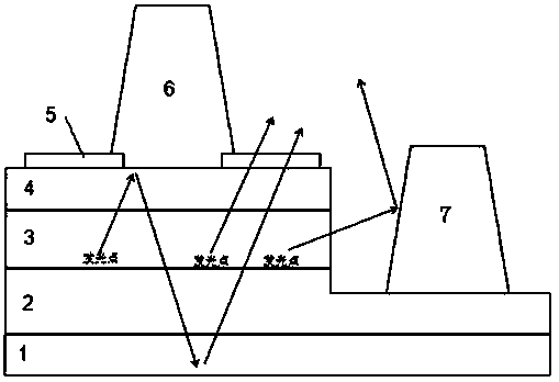
[0046] (1) Evaporation ITO thin film on the p-type GaN layer 4 of sapphire wafer 8 (GaN-based LED wafer) using electron beam evaporation table, the ITO thin film thickness is 600 angstroms, and annealing is carried out, and the sheet resistance obtained is lower than 30 ohms / Port, the ITO thin film layer with a transmittance greater than 85% (ie the ITO current spreading layer 5). Make a mask pattern through photoresist to obtain an ITO pattern, etch the N region to the n-type GaN layer 2 to form a mesa on the n-type GaN layer 2 .

[0047] (2) Making photolithographic electrode patterns to form a coated electrode structure

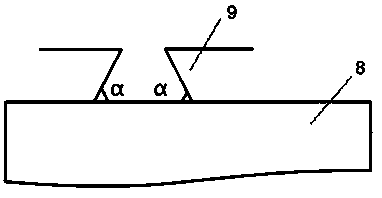
[0048] ① Coating: use negative photoresist 9 (see image 3 ) on the wafer surface to carry out the gluing step, the thickness of the gluing is 10000 angstroms, and the gluing speed is 1600rpm; the wafer that has been coated with gluing is placed on a hot plate (or other contact heating equipment) for preliminary drying (pre-baking), The temperature is t...

Embodiment 2

[0063] (1) With embodiment 1.

[0064] (2) Making photolithographic electrode patterns.

[0065] ①Glue application: use negative photoresist to apply glue on the surface of the wafer, the thickness of the glue is 35000 angstroms, and the speed of glue coating is 3000rpm; the coated wafer is preliminarily dried, and the temperature is controlled between 120°C. The time is between 120 seconds.

[0066] ②Exposure: Expose the wafer that has completed step ①. The exposure time is 25 seconds, and the exposure power is 500w.

[0067] ③Development: The wafer that has completed step ② is developed. The development time is 90 seconds, the temperature of the developer is 70°C, and the temperature is kept constant. After the development is completed, the wafer is baked for the third time. The temperature is 120°C and the time is 120 Second.

[0068] (3) Making electrode structure

[0069] 1. with embodiment 1;

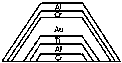
[0070] ② Evaporation of the first Cr layer: After the chamber reaches th...

Embodiment 3

[0077] Increase the thickness of the first Cr layer and the second Cr layer to 200 Angstroms.

[0078] (1) With embodiment 1.

[0079] (2) Making photolithographic electrode patterns

[0080] ① Glue coating: use negative photoresist to coat the surface of the wafer with a coating thickness of 20,000 angstroms and a speed of 2,000 rpm; preliminarily dry the coated wafer at a temperature of 100°C for 100 seconds .

[0081] ②Exposure: Expose the wafer that has completed step ①. The exposure time is 15 seconds, and the exposure power is 400w.

[0082] ③Development: The wafer that has completed step ② is developed. The development time is 70 seconds, the temperature of the developer is 60°C, and the temperature is kept constant. After the development is completed, the wafer is baked for the third time. The temperature is 120°C and the time is 120 Second.

[0083] (3) Making electrode structure

[0084] ① Same as Example 1.

[0085] ② Evaporation of the first Cr layer: After t...


PUM

PropertyMeasurementUnit
Thicknessaaaaaaaaaa
Thicknessaaaaaaaaaa
Thicknessaaaaaaaaaa

Abstract

A GaN-based LED electrode structure and a manufacturing method thereof are provided. A P electrode is arranged on an ITO (indium tin oxide) current extension layer; an N electrode is arranged on a terrace face of an n-type GaN layer; each of the P electrode and the N electrode structurally includes a first Cr layer, a first Al layer, a Ti layer, an Au layer, a second Cr layer and a second Al layersequentially from bottom to top. The manufacturing method herein includes the steps of (1) making an ITO film layer, and etching a terrace of an n-type GaN layer; (2) making a photoetched electrode pattern to form a coated electrode structure; (3) making the electrode structure. photoresist pattern chamfering is suitably controlled to implement the coated electrode structure; the reasonable electrode structure design ensures good viscosity for an electrode, and luminous efficiency of a die is greatly improved; the whole electrode structure is simple in design; a conventional evaporation material is applied to the whole structure; the overall manufacturing process takes short time and low cost; the Gan-based LED electrode structure is applicable to large-scale manufacturing of all GaN-based LED dies.

Description

technical field [0001] The invention relates to a GaN-based LED tube core with a high-reflectivity electrode structure and a specific manufacturing method thereof, belonging to the technical field of semiconductor processing. Background technique [0002] LED (Light Emitting Diode) is a device that relies on semiconductor P-N junctions for electroluminescence. It is made of compounds such as nitrogen, arsenic, gallium, and phosphorus. It can convert electrical energy into light energy through the recombination of electrons and holes. Radiant. Its basic structure is a piece of electroluminescent semiconductor material, which is a solid-state semiconductor device that can directly convert electricity into light. The LED is placed on a shelf with leads, and then sealed with epoxy resin around it. , It is beneficial to protect the internal core wire, so the shock resistance of LED is very good. At the same time, LED is widely recognized as the fourth-generation lighting source...

Claims


Application Information

Patent Timeline
IPC IPC(8): H01L33/36H01L33/40H01L33/32
CPCH01L33/32H01L33/36H01L33/405H01L2933/0016
Inventor 徐晓强刘琦闫宝华彭璐肖成峰
Owner SHANDONG INSPUR HUAGUANG OPTOELECTRONICS
Why Eureka
Try Eureka