Semiconductor device

a semiconductor device and semiconductor technology, applied in the field of semiconductor devices, can solve the problems of voltage resistance reduction of semiconductor devices, and achieve the effects of good reliability, good voltage resistance, and reduced voltage resistance of semiconductor devices

Active Publication Date: 2013-08-22
DENSO CORP
View PDF8 Cites 22 Cited by
  • Summary
  • Abstract
  • Description
  • Claims
  • Application Information

AI Technical Summary

Benefits of technology

[0008]According to this aspect, a decrease in voltage-resistance of the semiconductor device is able to be inhibited. The semiconductor device described above is thus able to achieve both good reliability and good voltage-resistance.

Problems solved by technology

As a result, the voltage-resistance of the semiconductor device may decrease.

Method used


Image

  • Semiconductor device
  • Semiconductor device
  • Semiconductor device

Examples


Embodiment Construction

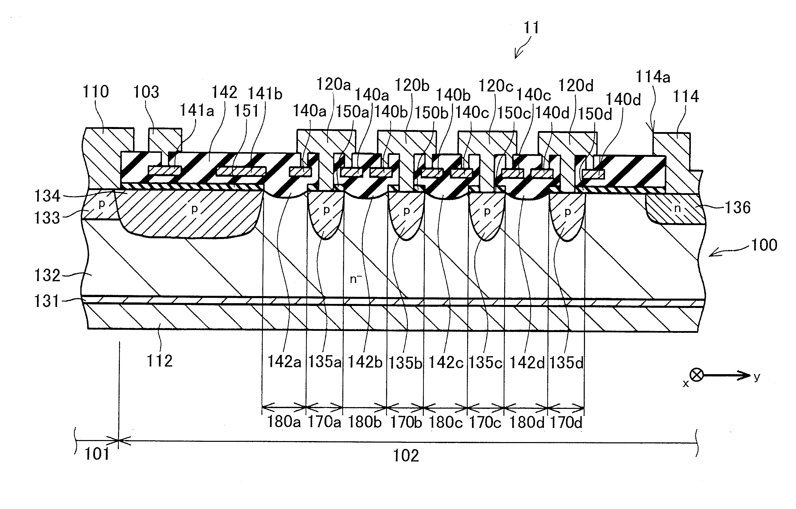
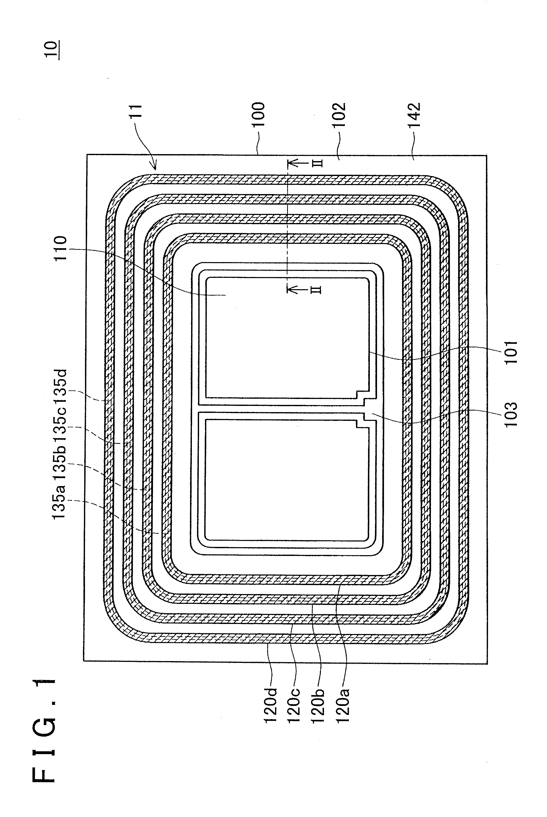
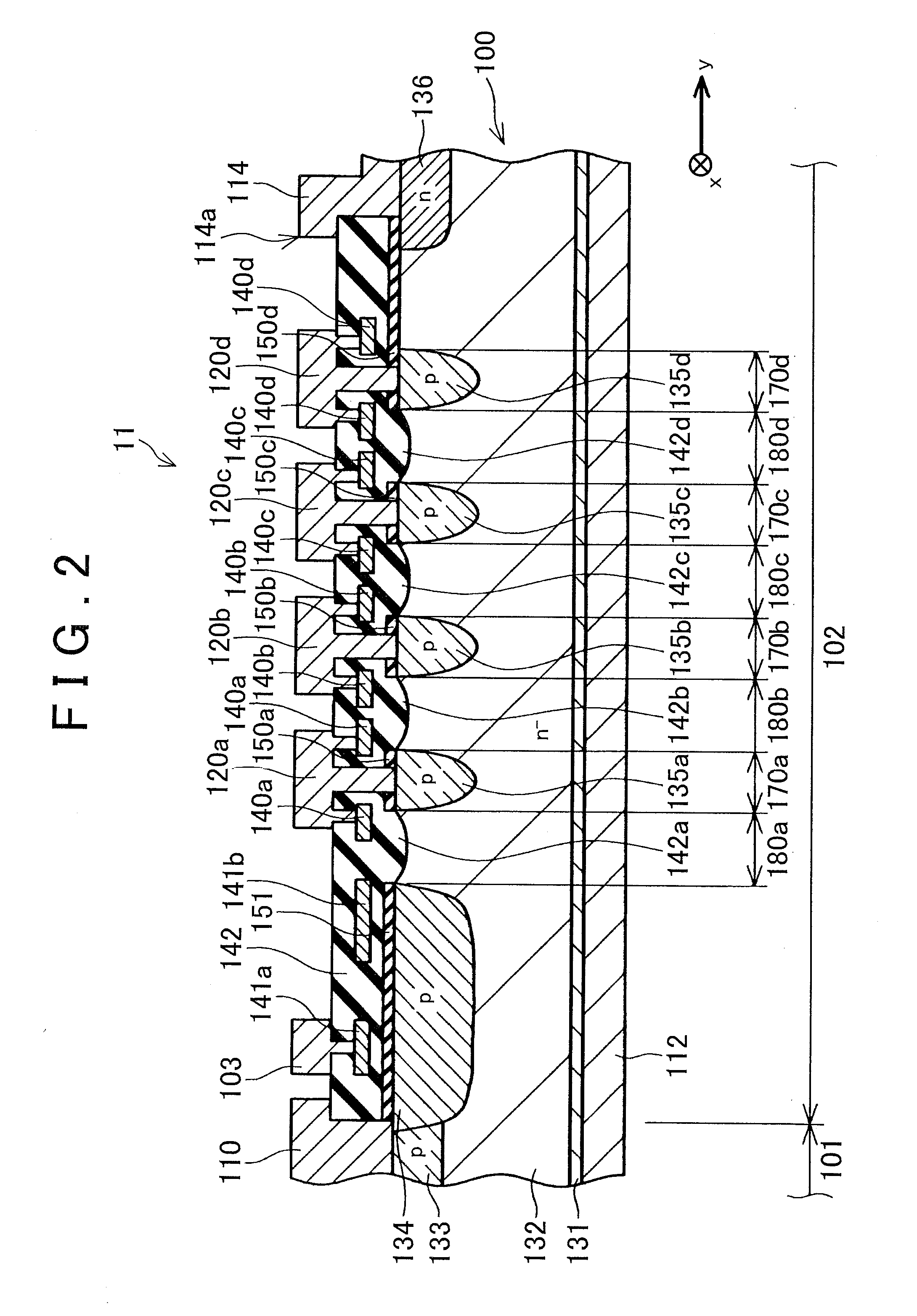
[0014]The semiconductor device of the invention is provided with a semiconductor substrate that has a cell region in which a semiconductor element is formed and a non-cell region provided around the cell region, and a field plate formed on a surface of the non-cell region. The semiconductor device may also be provided with a front surface electrode formed on a front surface of the cell region, and a back surface electrode formed on a back surface of the semiconductor substrate. The material of the front surface electrode is not limited, but a metal film the main component of which is aluminum (Al) or an aluminum-silicon alloy (AlSi) or the like may be used, for example. The material of the back surface electrode is not limited, but a stacked electrode in which Al or AlSi, titanium (Ti), nickel (Ni), and a nickel protective film of gold (Au) or the like, are stacked in order from the semiconductor substrate side, for example, may be used.

[0015]The non-cell region includes a first con...


PUM

PropertyMeasurementUnit
thicknessaaaaaaaaaa
conductiveaaaaaaaaaa
thicknessaaaaaaaaaa

Abstract

A field plate of a semiconductor device is provided with i) an insulating film that is formed on a surface of the semiconductor substrate, and includes a plurality of first regions, one for each of a plurality of FLR layers, that contact the layers and are arranged at intervals in a radial direction, and a plurality of second regions, one for each of the first regions, that are adjacent to the first regions in the radial direction, and ii) a plurality of first conductive films that are formed, one for each of the layers, inside of the insulating film, are arranged at intervals in the radial direction along the layers when a semiconductor substrate is viewed from above, and that are electrically connected to the layers. A thickness of at least a portion of the second regions is thicker than a thickness of the first regions.

Description

INCORPORATION BY REFERENCE[0001]The disclosure of Japanese Patent Application No. 2012-036416 filed on Feb. 22, 2012 including the specification, drawings and abstract is incorporated herein by reference in its entirety.BACKGROUND OF THE INVENTION[0002]1. Field of the Invention[0003]The invention relates to a semiconductor device.[0004]2. Description of Related Art[0005]In order to ensure voltage-resistance of a semiconductor device, a voltage-resistance retaining structure such as a field limiting ring layer (FLR layer) is formed in a peripheral region (a non-cell region) on a semiconductor substrate. Further, in order to ensure reliability of the semiconductor device, a field plate is formed on a front surface side of the FLR layer. Japanese Patent Application Publication No. 2009-38356 (JP 2009-38356 A) describes a semiconductor device in which a field plate that has a plurality of metal layers and a plurality of polysilicon layers is formed on a front surface side of each of a p...

Claims


Application Information

Patent Timeline
Patent Type & Authority Applications(United States)
IPC IPC(8): H01L29/02
CPCH01L29/02H01L29/402H01L29/404H01L29/7395H01L29/7811H01L29/408H01L29/0638H01L29/0657H01L29/0696H01L29/1095H01L29/0619
Inventor SENOO, MASARU
Owner DENSO CORP
Why Eureka
Try Eureka