Eureka AIR delivers breakthrough ideas for toughest innovation challenges, trusted by R&D personnel around the world.

Circuit layer manufacturing method and portable computer thereof

Active Publication Date: 2013-08-22
WISTRON CORP
View PDF6 Cites 2 Cited by
  • Summary
  • Abstract
  • Description
  • Claims
  • Application Information

AI Technical Summary

Benefits of technology

This patent uses a new design to create a more efficient and thin portable computer. The circuit board is directly formed on the front of the computer, eliminating the need for a separate substrate. This reduces space and thickness of the computer, allowing it to be more flexible in its use. The circuit board is fixed to the front without screws, and the control circuit layer is grounded to a flat region, reducing costs and simplifying assembly. Overall, this design improves the functionality and flexibility of portable computers while reducing costs and simplifying assembly.

Problems solved by technology

However, since the overall thickness of the control circuit board (including a substrate and a circuit layer formed on the substrate) is usually greater than 2.5 mm, the aforesaid assembly design is therefore disadvantageous to a slim design of the tablet computer and limits the structural design of the tablet computer and flexibility of the tablet computer in use of its inner space.
Thus, the aforesaid assembly design not only increases the component cost of the tablet computer in disposal of the control circuit board, but also causes a time-consuming and strenuous assembly process.

Method used


Image

  • Circuit layer manufacturing method and portable computer thereof
  • Circuit layer manufacturing method and portable computer thereof
  • Circuit layer manufacturing method and portable computer thereof

Examples


Embodiment Construction

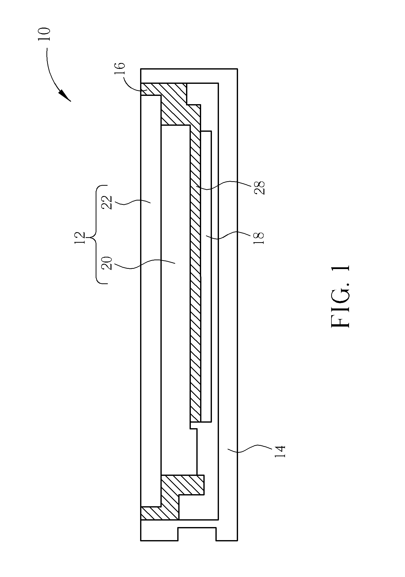
[0026]Please refer to FIG. 1, which is an inner front view of a portable computer 10 according to an embodiment of the present invention. As shown in FIG. 1, the portable computer 10 includes a display module 12, a back cover 14, a front bezel 16, and a circuit layer portion 18. The portable computer 10 can be a tablet computer, but not limited thereto, meaning that the portable computer 10 can also be other type of portable computer device, such as a notebook. In this embodiment, the display module 12 can include a display device 20 and a touch panel 22 (but not limited thereto). The display device 20 is disposed on the front bezel 16 for displaying images. The touch panel 22 is disposed on the display device 20 for providing a touch function. The front bezel 16 is connected to the back cover 14 for cooperatively containing the display module 12.

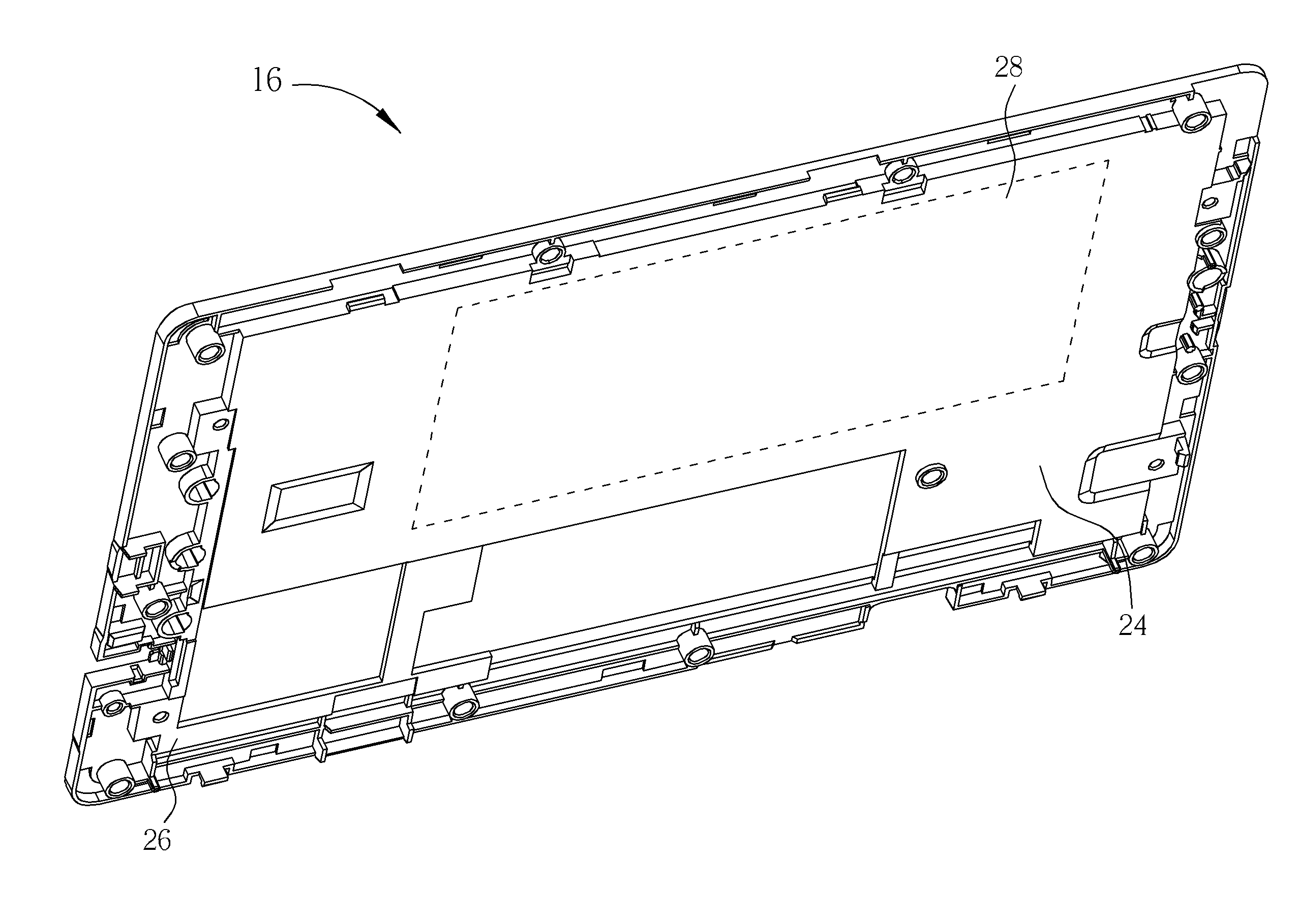
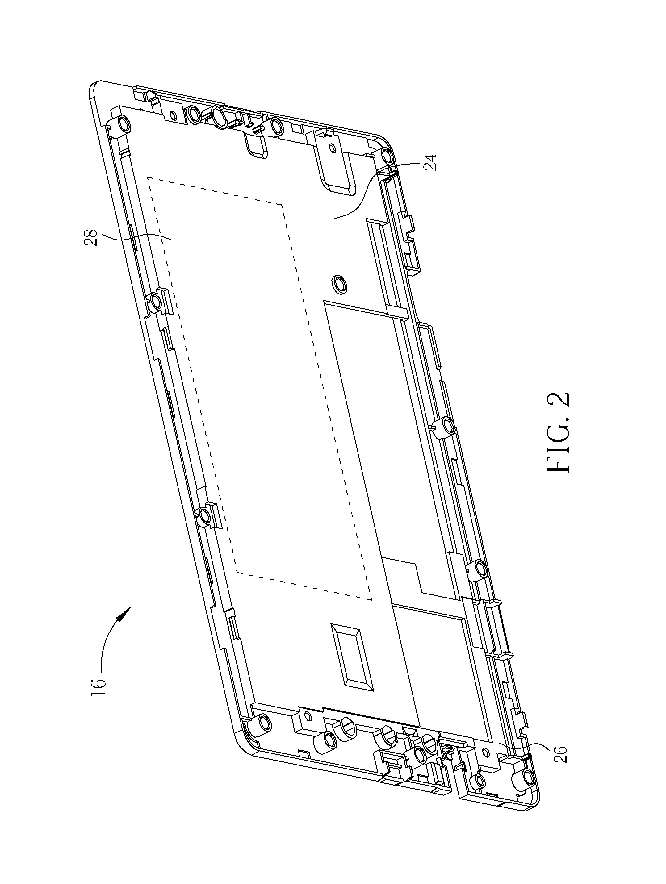
[0027]Next, please refer to FIG. 1 and FIG. 2. FIG. 2 is a diagram of the front bezel 16 in FIG. 1. As shown in FIG. 1 and FIG. 2, the fro...


PUM


Abstract

A circuit layer manufacturing method is applied to a portable computer. The portable computer includes a front bezel, a display module, and a back cover. The front bezel is connected to the back cover for containing the display module. The front bezel includes a metal portion. The metal portion has a flat region corresponding to a side of the back cover. The circuit layer manufacturing method includes forming at least one control circuit layer assembly on the flat region, grounding the control circuit layer assembly to the flat region, and forming a protection layer on the control circuit layer assembly. The control circuit layer assembly includes an insulation layer and a control circuit layer. The control circuit layer is electrically connected to the display module. The insulation layer is formed between the control circuit layer and the flat region for being alternately stacked with the control circuit layer.

Description

BACKGROUND OF THE INVENTION[0001]1. Field of the Invention[0002]The present invention relates to a circuit layer manufacturing method and a portable computer thereof, and more specifically, to a circuit layer manufacturing method of directly forming a circuit layer of a circuit board on a flat metal region of a front bezel of a portable computer to omit a substrate of the circuit board and a portable computer thereof.[0003]2. Description of the Prior Art[0004]With development of electronic technology, portable electronic apparatuses have made great progress on portability, and a tablet computer is one of the most representative examples.[0005]Generally speaking, in an assembly process of a tablet computer, first of all, a front bezel is utilized to hold a display device (e.g. a liquid crystal display panel) and a touch device, and a control circuit board and the front bezel with the display device and the touch device installed thereon are then installed on a back cover. Accordingly...

Claims


Application Information

Patent Timeline
IPC IPC(8): H05K3/10G06F1/16
CPCG06F1/1601G06F1/1626G06F1/1637G06F2200/1612H05K1/0215Y10T29/49126H05K2201/0999Y10T29/4913Y10T29/49117Y10T29/49165Y10T29/49155H05K1/056
Inventor WU, CHU-HSUN
Owner WISTRON CORP
Why Eureka
Eureka Blog
Learn More