Method of Applying a Pattern to a Substrate, Device Manufacturing Method and Lithographic Apparatus for Use in Such Methods

a technology of pattern and substrate, which is applied in the direction of photomechanical equipment, instruments, optics, etc., can solve the problems of increasing the unit cost of semiconductor or other products, limiting the throughput of lithography equipment, and still incurring overhead. , to achieve the effect of enhancing the second correction information

Active Publication Date: 2013-09-05
ASML NETHERLANDS BV
View PDF21 Cites 102 Cited by
  • Summary
  • Abstract
  • Description
  • Claims
  • Application Information

AI Technical Summary

Benefits of technology

[0035]The controller may be arranged automatically to process the measurements made after the substrate is loaded together with the results of the p

Problems solved by technology

Whichever type of apparatus is employed, the accurate placement of patterns on the substrate is a chief challenge for reducing the size of circuit components and other products that may be produced by lithography.
These operations, being time-consuming, limit the throughput of the lithography apparatus, and consequently increase the unit cost of the semiconductor or other products.
Nevertheless, an overhead is still incurred which limits the throughput that can be achieved.
These advanced models depend however on measuring an increased number of targets across the wafer, which is naturally more time-consuming, and further limits the thro

Method used


Image

  • Method of Applying a Pattern to a Substrate, Device Manufacturing Method and Lithographic Apparatus for Use in Such Methods
  • Method of Applying a Pattern to a Substrate, Device Manufacturing Method and Lithographic Apparatus for Use in Such Methods
  • Method of Applying a Pattern to a Substrate, Device Manufacturing Method and Lithographic Apparatus for Use in Such Methods

Examples


Embodiment Construction

[0051]The invention will be better understood from the following descriptions of various “embodiments” of the invention. Thus, specific “embodiments” are views of the invention, but each does not itself represent the whole invention. In many cases individual elements from one particular embodiment may be substituted for different elements in another embodiment carrying out a similar or corresponding function. It is expected that those skilled in the art with access to the teachings provided herein will recognize additional modifications, applications, and embodiments within the scope thereof and additional fields in which the invention would be of significant utility.

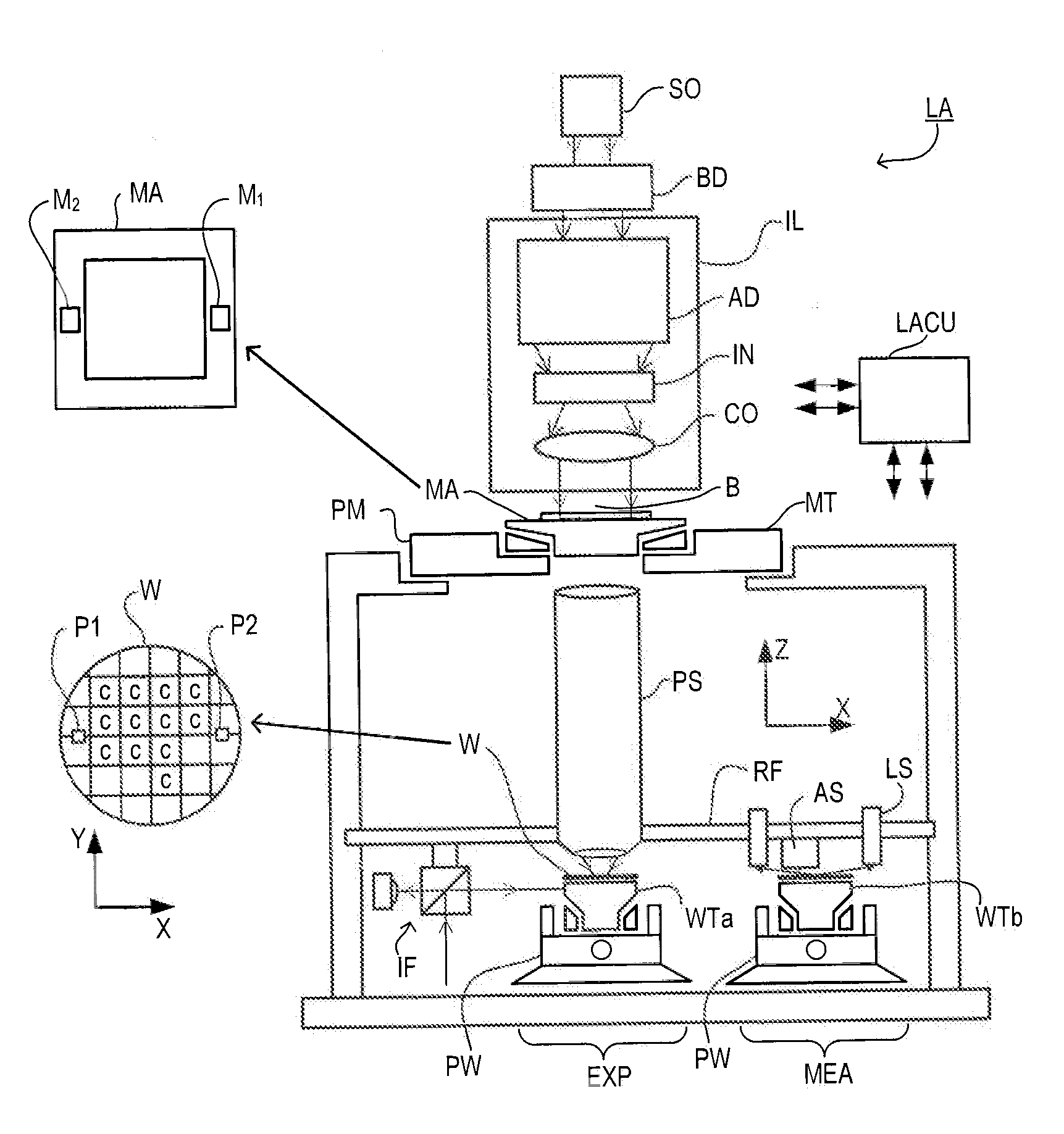
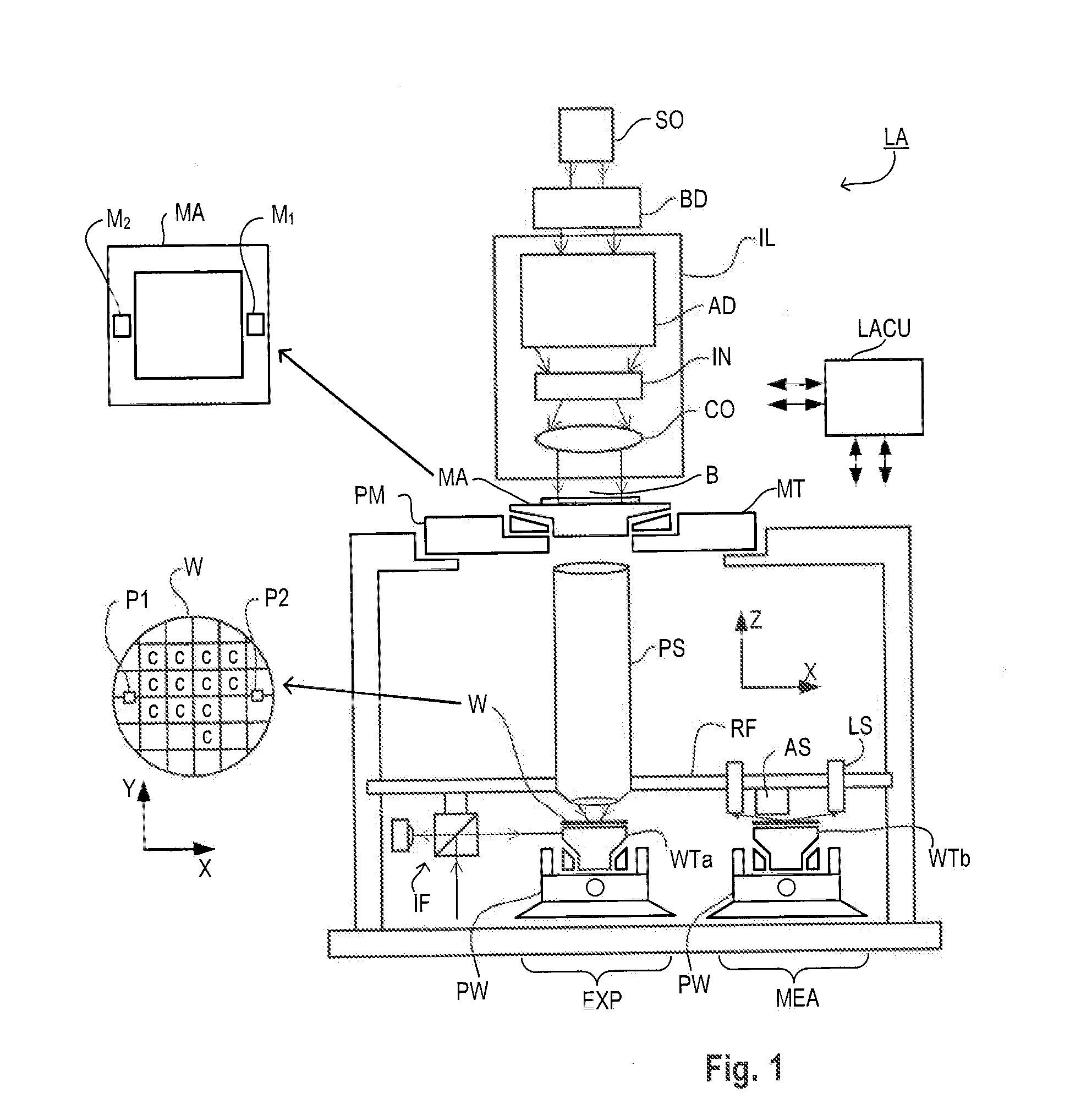
[0052]FIG. 1 schematically depicts a lithographic apparatus LA according to one embodiment of the invention. The apparatus comprises:[0053]an illumination system (illuminator) IL configured to condition a radiation beam B (e.g., UV radiation or EUV radiation).[0054]a support structure (e.g., a mask table) MT constructed...


PUM


Abstract

A substrate is loaded onto a substrate support of a lithographic apparatus, after which the apparatus measures locations of substrate alignment marks. These measurements define first correction information allowing the apparatus to apply a pattern at one or more desired locations on the substrate. Additional second correction information is used to enhance accuracy of pattern positioning, in particular to correct higher order distortions of a nominal alignment grid. The second correction information may be based on measurements of locations of alignment marks made when applying a previous pattern to the same substrate. The second correction information may alternatively or in addition be based on measurements made on similar substrates that have been patterned prior to the current substrate.

Description

CROSS REFERENCE TO RELATED APPLICATIONS[0001]This application claims the benefit under 35 U.S.C. §119(e) to U.S. Provisional Patent Application No. 61 / 540,161, filed Sep. 28, 2011, which is incorporated by reference herein in its entirety.BACKGROUND[0002]1. Field of the Invention[0003]The invention relates to method of transferring a pattern from a patterning device onto a substrate using a lithographic apparatus, to a device manufacturing method. The invention further relates to a lithographic apparatus constructed and arranged to carry out the method, and to a computer program product for controlling a lithographic apparatus to implement steps of the method.[0004]2. Related Art[0005]A lithographic apparatus is a machine that applies a desired pattern onto a substrate, usually onto a target portion of the substrate. A lithographic apparatus can be used, for example, in the manufacture of integrated circuits (ICs). In that instance, a patterning device, which is alternatively referr...

Claims


Application Information

Patent Timeline
IPC IPC(8): G03F7/20
CPCG03F7/70141G03F9/7088G03F7/70633G03F9/7003H01L21/0274G03F7/70616
Inventor VAN DER SANDEN, STEFAN CORNELIS THEODORUSVAN HAREN, RICHARD JOHANNES FRANCISCUSIMONS, HUBERTUS JOHANNES GERTRUDUSEDART, REMI DANIEL MARIEWEI, XIUHONGKUBIS, MICHAELLYULINA, IRINA
Owner ASML NETHERLANDS BV
Why Eureka
Try Eureka