Semiconductor device

a technology of semiconductors and semiconductors, applied in the direction of semiconductor devices, electrical equipment, transistors, etc., can solve the problems of deterioration achieve the effects of suppressing the change of the electrical characteristics of the transistor, high resistance to chemical liquid, and high barrier property against impurities

Inactive Publication Date: 2013-09-12
SEMICON ENERGY LAB CO LTD
View PDF5 Cites 24 Cited by
  • Summary
  • Abstract
  • Description
  • Claims
  • Application Information

AI Technical Summary

Benefits of technology

[0020]The aluminum oxide film is provided over the crystalline insulating film, whereby the aluminum oxide film can have crystallinity and a density greater than or equal to 3.2 g/cm3 and less than or equal to 4.1 g/cm3. The aluminum oxide film has a high barrier property against impurities. Accordingly, a change in electrical characteristics of a transistor, which is caused by impurities, can be suppressed.
[0021]Further, the aluminum oxide film having a density greater than or equal to 3.2 g/cm3 and less than or equal to 4.1 g/cm3 has high resistance to a chemical liquid, plasma, or the like and is not unintentionally etched with ease. Therefore, occurrence of shape defects of the aluminum oxide film, which is caused by unintentional etching, can be suppressed. Note that in portions where shape defects of layers that constitute a transistor occur, an etching residue occurs and another shape defect is caused by the portion. Thus, it is important to suppress occurrence of shape defects in order to provide transistor having stable e

Problems solved by technology

In the case where glass is used as a substrate over which the transistor is provided, the electrica

Method used


Image

  • Semiconductor device
  • Semiconductor device
  • Semiconductor device

Examples


embodiment 1

[0091]In this embodiment, a transistor of one embodiment of the present invention will be described.

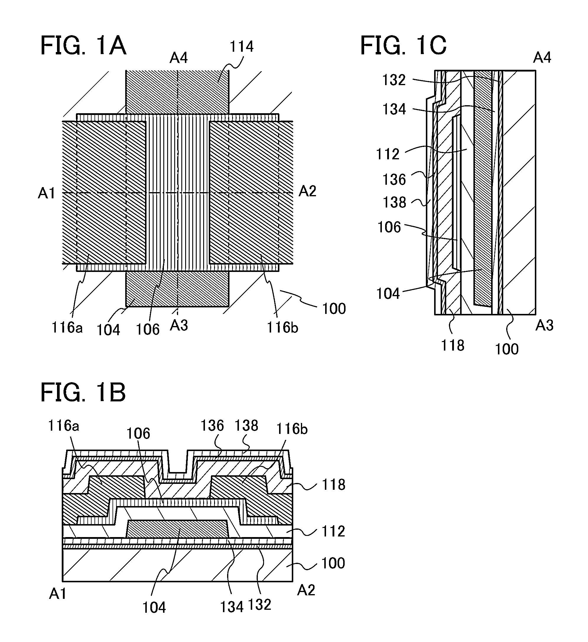
[0092]FIG. 1A is a top view of a transistor of one embodiment of the present invention. FIG. 1B is a cross-sectional view taken along dashed-dotted line A1-A2 in FIG. 1A. FIG. 1C is a cross-sectional view taken along dashed-dotted line A3-A4 in FIG. 1A. Note that for simplicity, a gate insulating film 112 and the like are not illustrated in FIG. 1A.

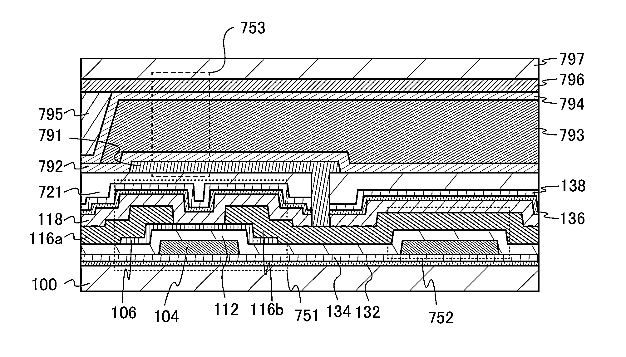
[0093]FIG. 1B is a cross-sectional view of a transistor including a crystalline insulating film 132 over a substrate 100; an aluminum oxide film 134 over the crystalline insulating film 132; a gate electrode 104 over the aluminum oxide film 134; the gate insulating film 112 over the gate electrode 104; a semiconductor film 106 which is over the gate insulating film 112 and overlaps with the gate electrode 104; a source electrode 116a and a drain electrode 116b over the semiconductor film 106; a crystalline insulating film 136 over the semic...

embodiment 2

[0271]In this embodiment, methods for manufacturing the transistors described in Embodiment 1 will be described.

[0272]First, a method for manufacturing the transistor illustrated in FIGS. 1A to 1C will be described with reference to FIGS. 7A to 7D and FIGS. 8A to 8C. Note that only cross-sectional views corresponding to FIG. 1B are shown for simplicity in FIGS. 7A to 7D and FIGS. 8A to 8C.

[0273]First, the substrate 100 is prepared. As the substrate 100, a substrate selected from the substrates given as examples of the substrate 100 can be used.

[0274]Next, the crystalline insulating film 132 is formed (see FIG. 7A). The crystalline insulating film 132 can be formed using an insulating film selected from the insulating films given as examples of the crystalline insulating film 132 and can be formed by a sputtering method, a chemical vapor deposition (CVD) method, a molecular beam epitaxy (MBE) method, an atomic layer deposition (ALD) method, or a pulsed laser deposition (PLD) method. ...

embodiment 3

[0437]In this embodiment, a transistor of one embodiment of the present invention will be described.

[0438]FIG. 20A is a top view of a transistor of one embodiment of the present invention. FIG. 20B is a cross-sectional view taken along dashed-dotted line G1-G2 in FIG. 20A. FIG. 20C is a cross-sectional view taken along dashed-dotted line G3-G4 in FIG. 20A. Note that for simplicity, a gate insulating film 2112 and the like are not illustrated in FIG. 20A.

[0439]FIG. 20B is a cross-sectional view of a transistor including a gate electrode 2104 over a substrate 2100; the gate insulating film 2112 over the gate electrode 2104; a semiconductor film 2106 which is over the gate insulating film 2112 and overlaps with the gate electrode 2104; a source electrode 2116a and a drain electrode 2116b over the semiconductor film 2106; and a protective insulating film 2118 over the semiconductor film 2106, and the source electrode 2116a and the drain electrode 2116b. Note that the gate insulating fil...


PUM


Abstract

A semiconductor device which has stable electrical characteristics and high reliability is provided. The semiconductor device includes a gate electrode over an insulating surface, a gate insulating film over the gate electrode, a semiconductor film which is over the gate insulating film and overlaps with the gate electrode, and a protective insulating film over the semiconductor film; and the protective insulating film includes a crystalline insulating film and an aluminum oxide film over the crystalline insulating film.

Description

BACKGROUND OF THE INVENTION[0001]1. Field of the Invention[0002]The present invention relates to a semiconductor device and a manufacturing method thereof.[0003]In addition, the present invention relates to an object, a method, a method for producing an object, a process, a machine, manufacture, or a composition of matter. In particular, the present invention relates to, for example, a semiconductor device, a memory device, a display device, a liquid crystal display device, a light-emitting device, a driving method thereof, or a manufacturing method thereof. Alternatively, the present invention relates to, for example, an electronic device including the memory device, the display device, or the light-emitting device.[0004]Note that in this specification, a semiconductor device refers to any device that can function by utilizing semiconductor characteristics, and an electro-optical device, a semiconductor circuit, an electronic device, and the like are all semiconductor devices.[0005...

Claims


Application Information

Patent Timeline
IPC IPC(8): H01L29/786
CPCH01L29/786H01L29/7869
Inventor TANAKA, TETSUHIROTAKAHASHI, ERIKA
Owner SEMICON ENERGY LAB CO LTD
Why Eureka
Try Eureka