Unlock instant, AI-driven research and patent intelligence for your innovation.
Method of redistributing functional element
Inactive Publication Date: 2013-09-12
NEC CORP +1
View PDF9 Cites 21 Cited by
Summary
Abstract
Description
Claims
Application Information
AI Technical Summary
This helps you quickly interpret patents by identifying the three key elements:
Problems solved by technology
Method used
Benefits of technology
Benefits of technology
This patent is about a method of creating a functionally-redistributed semiconductor device. The method involves adding an insulating layer to a functional element and then flattening the surface using a sacrificial layer. This helps to prevent damage to the internal interconnection structure of the element and ensures high reliability and yield. The method also allows for a fine interconnection conductive layer to be formed with high flatness after removal of the sacrificial layer. Overall, this patent provides a solution for improving the efficiency and reliability of semiconductor device production.
Problems solved by technology
However, the aforementioned technology disclosed in the patent documents has the following problems.
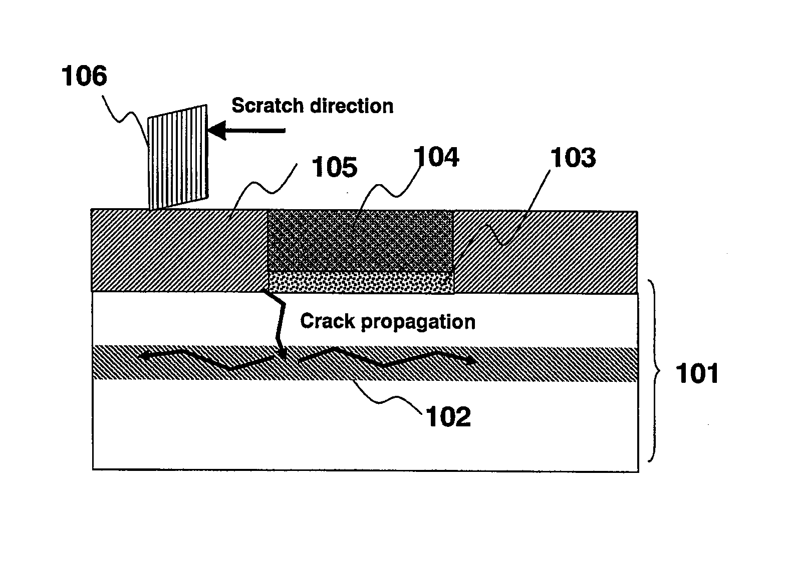
A first problem is that stress is applied to a circuit layer within a semiconductor device during a surface flattening process.
As a result, a low-k layer (interlayer dielectric having a low dielectric constant) 102 is problematically broken.
Furthermore, defects such as crack are produced inside of the semiconductor device, resulting in poor reliability of a product.
A second problem is that the manufacturing yield is lowered by open defects produced after the formation of the interconnection conductive layer because a seed layer is discontinuously formed at some locations.
Accordingly, when an interconnection is formed with a width of 20 μm or less and a thickness of 20 μm or less, patterning defects are likely to occur in exposure and development of a photoresist, resulting in a lowered manufacturing yield.
Thus, the manufacturing yield is problematically lowered by open defects produced after the formation of the interconnection conductive layer.
Method used
Image
Click on the blue label to locate the original text in one second.
Reading with bidirectional positioning of images and text.
Examples
first embodiment
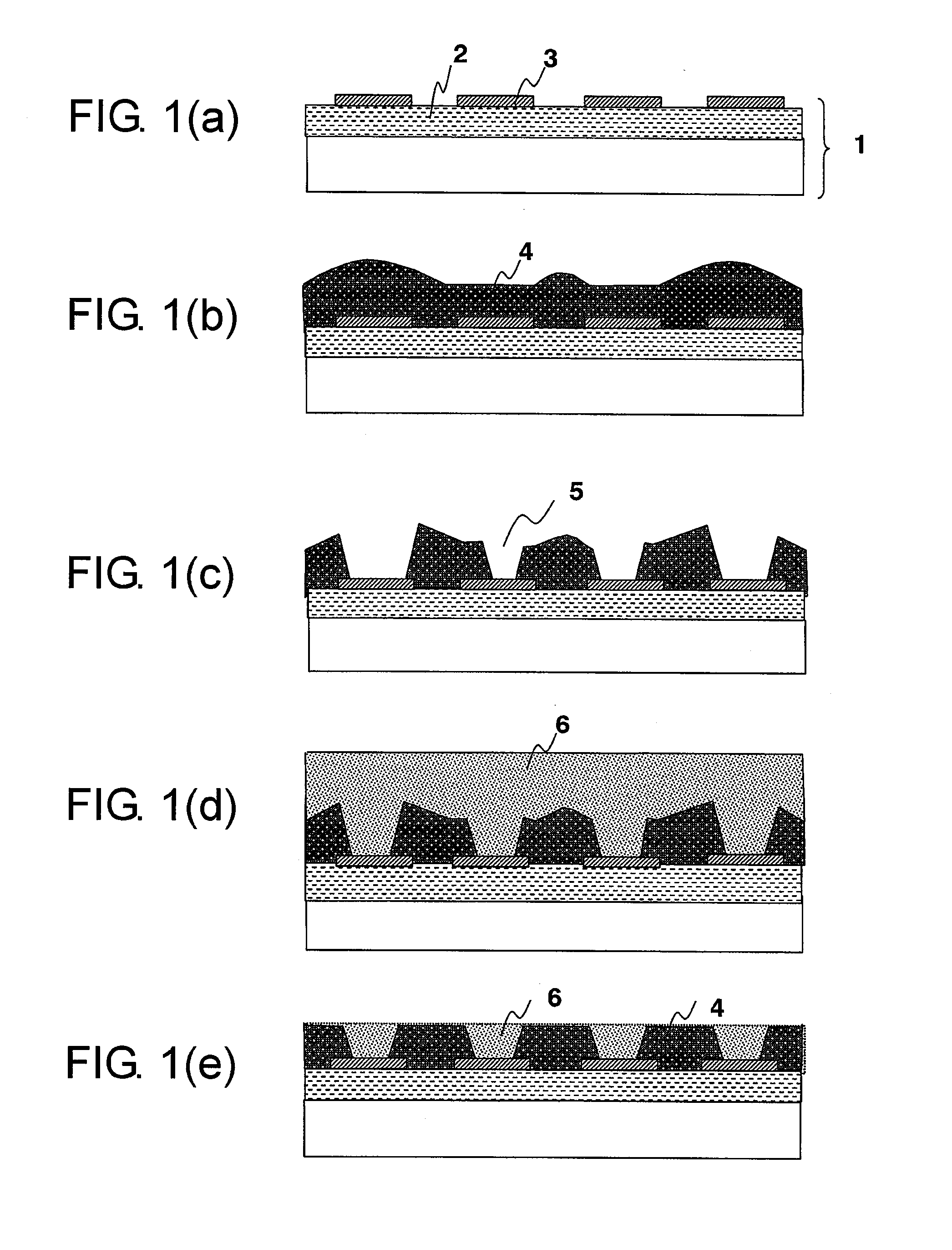
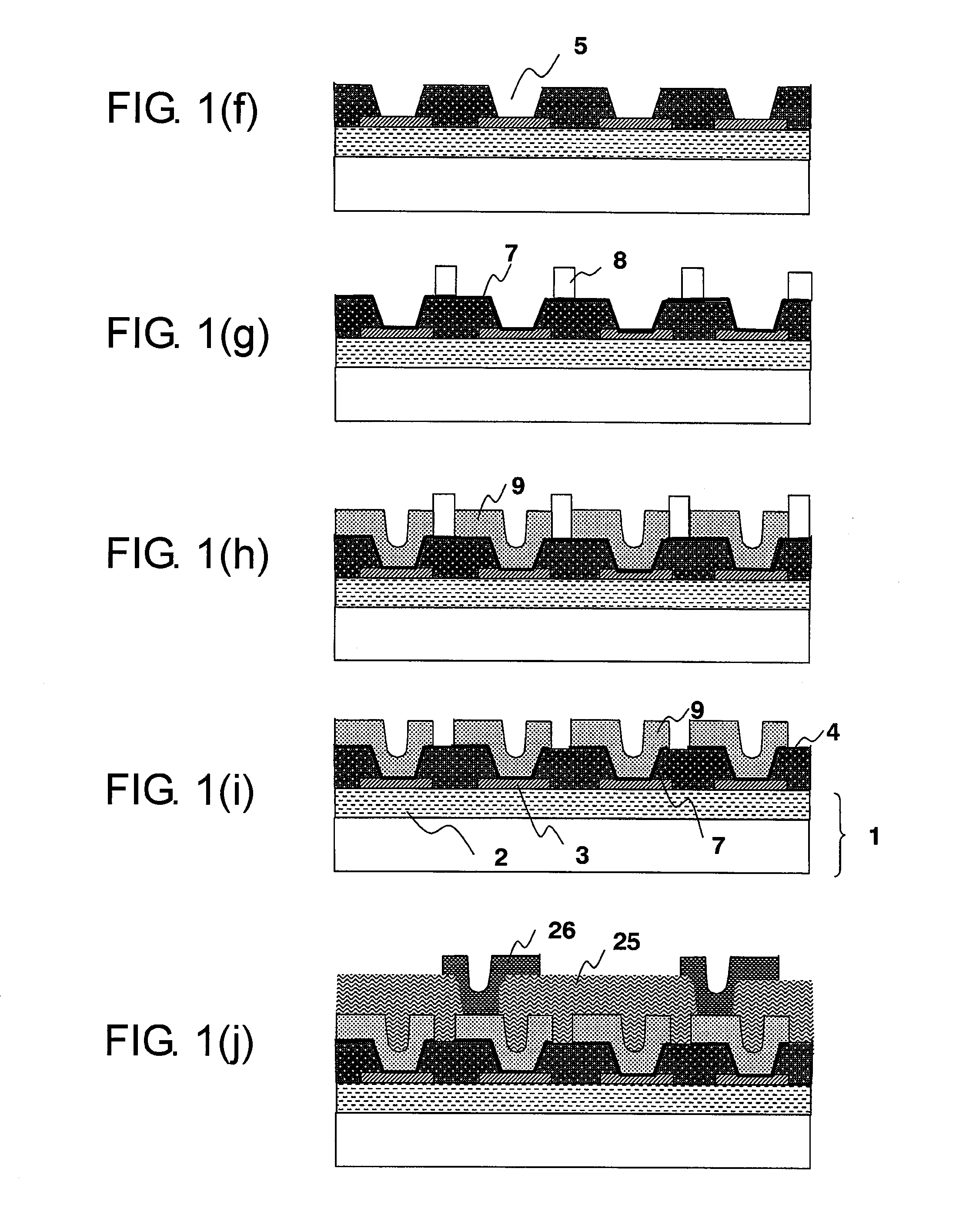
[0051]Embodiments of the present invention will be described in detail with reference to the drawings. FIGS. 1(a) to 1(e) and 1(f) to 1(j) are schematic cross-sectional views showing processes of a manufacturing method according to a first embodiment of the present invention.
[0052]FIG. 1(a) shows a structure of a functional element 1, an internal interconnection layer 2 of the functional element, and electrode pads 3 provided on the uppermost portion of the internal interconnection layer 2. In FIG. 1(b), an insulating layer 4 is formed. A spin coating method, a curtain coating method, a printing method, a laminating method, and the like are suitably used to supply the insulating layer 4. However, the method of supplying the insulating layer 4 is not limited to those specific examples. Then, for example, in a case where the insulating layer 4 is formed of an insulating resin layer, resin may be cured as needed with an oven, a hot plate, or the like. Inorganic substance can be used fo...
second embodiment
[0061]FIGS. 2(a) to 2(e) and 2(f) to 2(j) are schematic cross-sectional views showing processes of a manufacturing method according to a second embodiment of the present invention.
[0062]FIG. 2(a) shows a structure in which, after an interconnection layer 12 is formed on a base substrate 11, metal pillars 13 are formed on the interconnection layer 12. Metals such as Cu and stainless, glass substrates, alumina substrates, Si, and the like are suitably used for the base substrate according to the present invention. However, the material of the base substrate is not limited to those specific examples. Furthermore, from the viewpoint of electric characteristics, it is preferable to provide an insulating layer between the base substrate 11 and the interconnection layer 12 in a case where the base substrate 11 is a conductor or a semiconductor. In a case where the base substrate 11 is a functional element, the metal pillars 13 provided right above electrode pads via the interconnection lay...
third embodiment
[0074]FIGS. 3(a) to 3(d) and 3(e) to 3(h) are schematic cross-sectional views showing processes of a manufacturing method according to a third embodiment of the present invention.
[0075]FIG. 3(a) shows a structure which includes a functional element 31, an internal interconnection layer 32 of the functional element, and electrode pads 33 provided on the uppermost layer of the internal interconnection layer 32. In FIG. 3(b), sacrificial layers pillars 34 are made of organic resin. The sacrificial layer pillars are formed on the electrode pads 33. In a case where the sacrificial layer pillars 34 are made of a photosensitive material, the sacrificial layer pillars 34 can be formed by exposure and development. In a case where the sacrificial layer pillars 34 are made of a non-photosensitive material, the sacrificial layer pillars 34 can be formed by a printing method. However, the method of forming the sacrificial layer pillars 34 is not limited to those specific examples. In a case wher...
PUM
Abstract
According to a method of redistributing a functional element of the present invention, an insulating resin layer is supplied onto a functional element wafer such as an LSI. A portion to be a via hole on an electrode pad of the functional element is filled with a sacrificial layer. The top of the sacrificial layer filled in the via hole is exposed from the insulating layer by grinding or polishing. Therefore, it is possible to prevent breakage of a brittle material such as a low-k material in the functional element, which would be caused by transmission of shearing stress when a conventional pillar or a conventional gold projecting electrode is used. The reliability, the yield, and the level of flatness can be improved by forming an interconnection conductive layer after the flattening process of grinding or polishing. Accordingly, a fine conductive interconnection can be formed.
Description
TECHNICAL FIELD[0001]The present invention relates to a method of redistributing or rewiring a functional element, and more particularly to a method of redistributing or rewiring a functional element that can reduce influence of stress produced in an internal element during a surface flattening process.BACKGROUND ART[0002]Recent functional elements have been miniaturized with improved performance and advanced functions. A redistribution conductive layer has been added to a miniaturized functional element in order to rewire the functional element and to achieve a higher packaging density. Thus, size reduction of electronic equipment has been achieved. It is to be noted throughout the instant specification that the term “redistributing” is used to specify rewiring for repetition of wiring.[0003]The following patent documents disclose a method of redistributing or rewiring a functional element. For example, Japanese Patent No. 4057146 and Japanese laid-open patent publication No. 2007-...
Claims
Application Information
Patent Timeline
Application Date:The date an application was filed.
Publication Date:The date a patent or application was officially published.
First Publication Date:The earliest publication date of a patent with the same application number.
Issue Date:Publication date of the patent grant document.
PCT Entry Date:The Entry date of PCT National Phase.
Estimated Expiry Date:The statutory expiry date of a patent right according to the Patent Law, and it is the longest term of protection that the patent right can achieve without the termination of the patent right due to other reasons(Term extension factor has been taken into account ).
Invalid Date:Actual expiry date is based on effective date or publication date of legal transaction data of invalid patent.
