Heat treatment apparatus for heating substrate by light irradiation

a technology of heat treatment apparatus and electronic substrate, which is applied in the direction of laser beam welding apparatus, welding/soldering/cutting articles, manufacturing tools, etc., can solve the problems of increasing the size of the chamber, and affecting the quality of the substra

Active Publication Date: 2013-09-26
DAINIPPON SCREEN MTG CO LTD
View PDF66 Cites 45 Cited by
  • Summary
  • Abstract
  • Description
  • Claims
  • Application Information

AI Technical Summary

Benefits of technology

[0015]This can prevent the infrared-transparent window from being heated by radiation heat generated from the substrate, which may otherwise cause the infrared-transparent window to be opaque to the infrared ray.

Problems solved by technology

Providing a wafer rotation mechanism in the chamber complicates a configuration of the apparatus and increases the size of the chamber.
In addition, a problem arises that particles are inevitably generated from the rotation mechanism and scattered within the chamber.
Therefore, it is impossible to detect local non-uniformity in the temperature distribution.
Performing the feed-back control on the output of the halogen lamps based on such a measurement result may cause concentric non-uniformity in the temperature distribution.
This makes it likely that a temperature abnormality occurs particularly in the peripheral portion of the semiconductor wafer, which may cause warping of the wafer.

Method used


Image

  • Heat treatment apparatus for heating substrate by light irradiation
  • Heat treatment apparatus for heating substrate by light irradiation
  • Heat treatment apparatus for heating substrate by light irradiation

Examples


first preferred embodiment

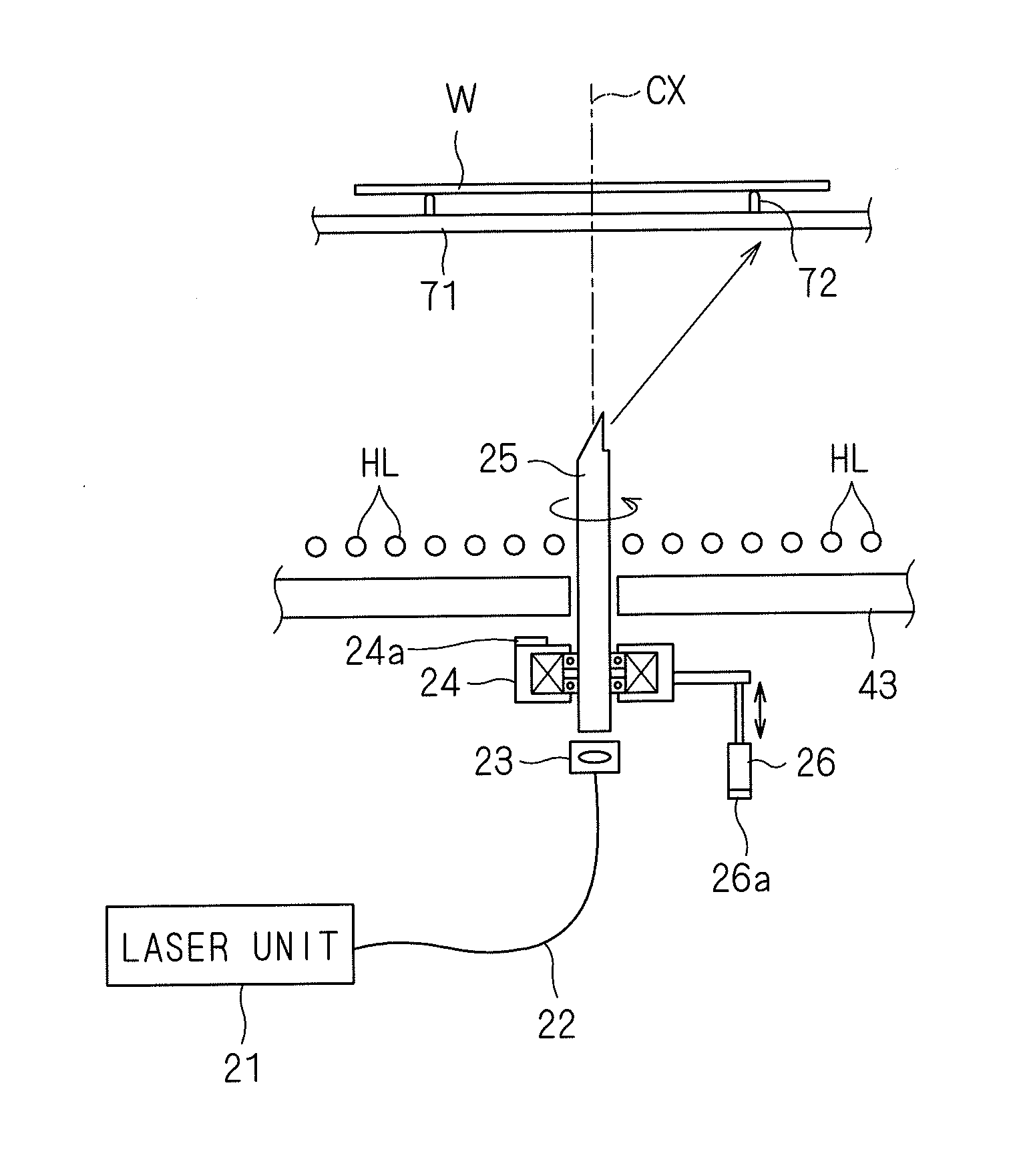
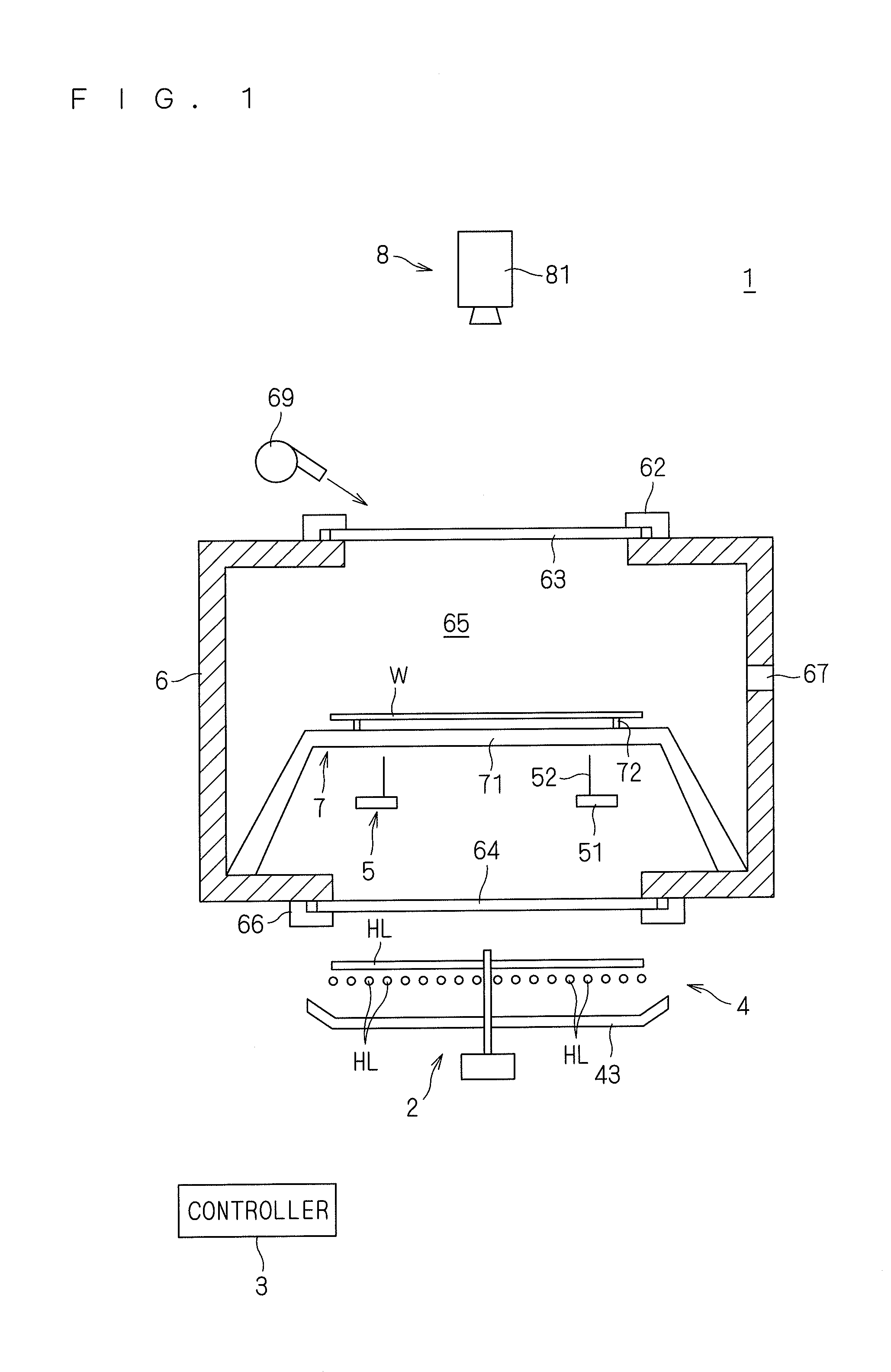
[0030]FIG. 1 is a diagram showing a configuration of principal parts of a heat treatment apparatus 1 according to the present invention. The heat treatment apparatus 1 is a lamp annealer that performs a heat treatment (back side annealing) on a substantially circular semiconductor wafer W by irradiating a back surface of the semiconductor wafer W with light. In FIG. 1 and subsequent Figures, the dimensions of components and the number of components are shown in an exaggerated or simplified form, as appropriate, for the sake of easier understanding.

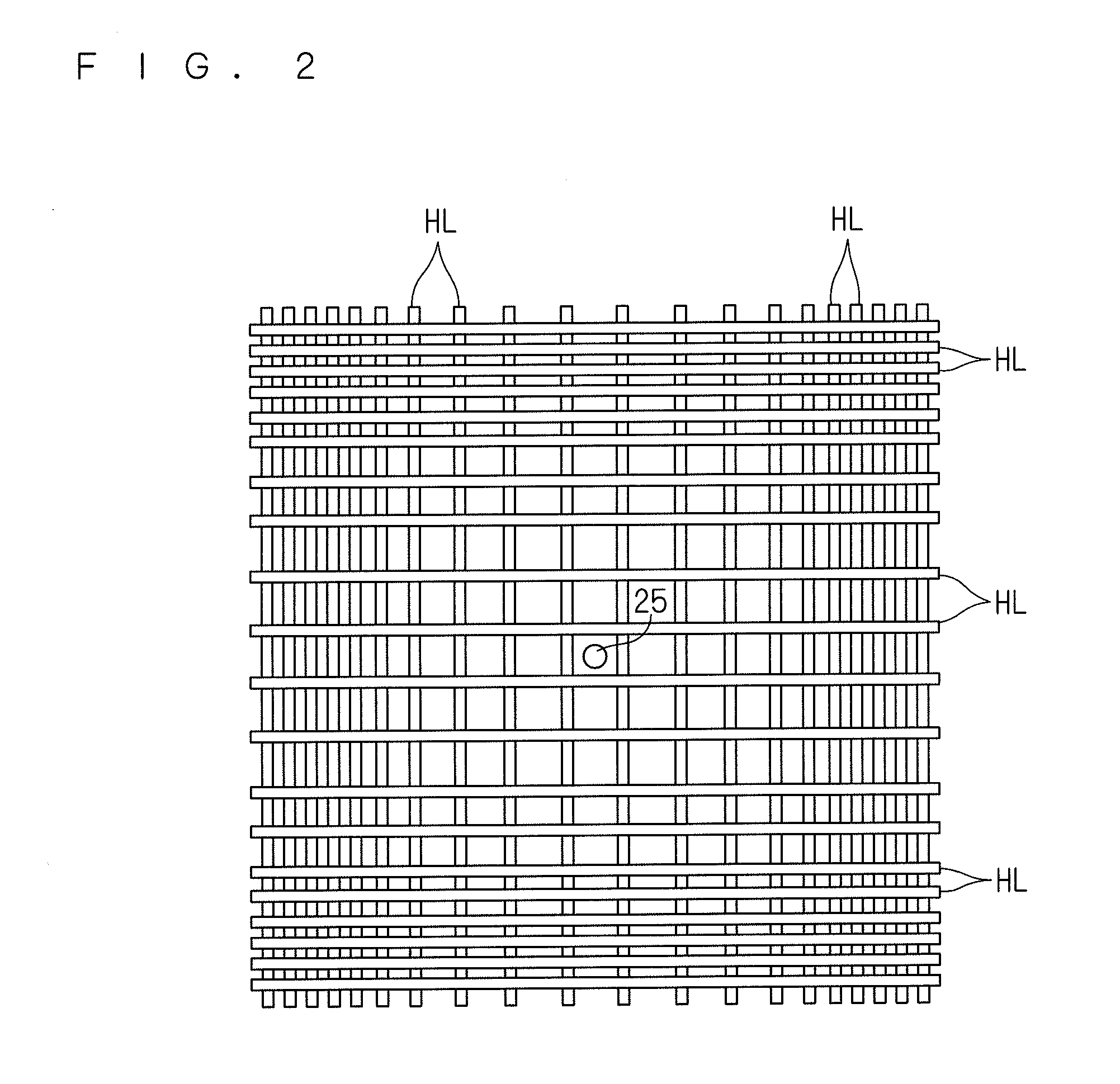
[0031]The heat treatment apparatus 1 principally includes a chamber 6, a holder 7, a light irradiation part 4, a temperature detection part 8, and a temperature correction part 2. The chamber 6 has a substantially cylindrical shape, and receives the semiconductor wafer W therein. The holder 7 holds the semiconductor wafer W within the chamber 6. The light irradiation part 4 irradiates the semiconductor wafer W held on the holder 7 with lig...

second preferred embodiment

[0083]Next, a second preferred embodiment of the present invention will be described. FIG. 10 is a diagram conceptually showing a situation of a temperature correction in a heat treatment apparatus 1a according to the second preferred embodiment. In FIG. 10, the same parts as those of the first preferred embodiment are denoted by the same corresponding reference numerals. The heat treatment apparatus 1a according to the second preferred embodiment is the same as the heat treatment apparatus 1 according to the first preferred embodiment, except for the configuration of the temperature detection part 8.

[0084]In the second preferred embodiment, the temperature detection part 8 includes a laser light receiving part 85 and a light receiving unit 86. The laser light receiving part 85 is a rod-shaped optical member made of quartz, which is identical to the laser light emission part 25. The laser light receiving part 85 is the laser light emission part 25 being placed upside down. A rotatio...

third preferred embodiment

[0091]Next, a third preferred embodiment of the present invention will be described. FIG. 11 is a diagram showing a configuration of principal parts of a heat treatment apparatus 1b according to the third preferred embodiment. In FIG. 11, the same parts as those of the first preferred embodiment are denoted by the same corresponding reference numerals. In the heat treatment apparatus 1b according to the third preferred embodiment, an infrared-transparent window 163 is arranged at a higher position and at a longer distance from the semiconductor wafer W as compared with the infrared-transparent window 63 of the first preferred embodiment.

[0092]In the third preferred embodiment, an upper wall 166 is provided at an upper end portion of the side wall of the chamber 6. The upper wall 166 is in the shape of a circular truncated cone. The upper wall 166 is made of, for example, stainless steel having an excellent heat resistance, and cooled by a water-cooling mechanism (not shown). The inf...


PUM

PropertyMeasurementUnit
distanceaaaaaaaaaa
thicknessaaaaaaaaaa
wavelengthaaaaaaaaaa

Abstract

The temperature of a semiconductor wafer is raised by light irradiation heating performed by halogen lamps. An infrared ray emitted from the semiconductor wafer whose temperature has been raised transmits through an infrared-transparent window made of silicon, and then is detected by an infrared camera. The infrared camera two-dimensionally detects the temperature of an entire surface of the semiconductor wafer. Based on a result of the detection obtained by the infrared camera, a temperature drop region having a relatively low temperature among the region of the semiconductor wafer is irradiated with laser light emitted from a laser light emission part. Accordingly, without rotating the semiconductor wafer, a temperature distribution can be made uniform with a high accuracy throughout the entire surface of the semiconductor wafer.

Description

BACKGROUND OF THE INVENTION[0001]1. Field of the Invention[0002]The present invention relates to a heat treatment apparatus for heating a thin plate-like precision electronic substrate (hereinafter, simply referred to as “substrate”), such as a semiconductor wafer and a glass substrate for a liquid crystal display device, by irradiating the substrate with light.[0003]2. Description of the Background Art[0004]Conventionally, in a process for manufacturing a semiconductor device and the like, various types of heat treatments are performed on a substrate such as a semiconductor wafer. As a heat treatment method on the semiconductor wafer, a rapid thermal process (RTP) has been in wide use. In a typical RTP apparatus, a semiconductor wafer held in a chamber is irradiated with light emitted from halogen lamps, so that the temperature of the semiconductor wafer is raised to a predetermined processing temperature in a short time of about several seconds. Rapidly raising the temperature of ...

Claims


Application Information

Patent Timeline
Patent Type & Authority Applications(United States)
IPC IPC(8): B23K26/00
CPCH01L21/324B23K26/0066H01L21/67248B23K26/127H01L21/67115B23K26/0042B23K26/0006B23K2103/56B23K26/50H01L21/26B23K26/352
Inventor KUSUDA, TATSUFUMI
Owner DAINIPPON SCREEN MTG CO LTD
Why Eureka
Try Eureka