Signal processing circuit, signal processing method, optical receiver and optical communication system

a signal processing and signal technology, applied in multiplex communication, electrical equipment, electromagnetic transmission, etc., can solve the problems of inability to know the value of the optical phase deviation in advance, and the frequency of the optical carrier wave of the signal light and the frequency of the local light are not identical perfectly, so as to reduce the influence of noise and improve accuracy.

Active Publication Date: 2013-09-26
NEC CORP
View PDF0 Cites 26 Cited by
  • Summary
  • Abstract
  • Description
  • Claims
  • Application Information

AI Technical Summary

Benefits of technology

[0039]The present invention has an effect that the present invention makes it possible to reduce influence of noise which is caused by a phase deviation and to calculate an amount of phase compensation with superior accuracy.

Problems solved by technology

However, in general, the frequency of the optical carrier wave of the signal light and the frequency of the local light are not identical perfectly.
It is impossible to know a value of the optical phase deviation in advance.

Method used


Image

  • Signal processing circuit, signal processing method, optical receiver and optical communication system
  • Signal processing circuit, signal processing method, optical receiver and optical communication system
  • Signal processing circuit, signal processing method, optical receiver and optical communication system

Examples


first exemplary embodiment

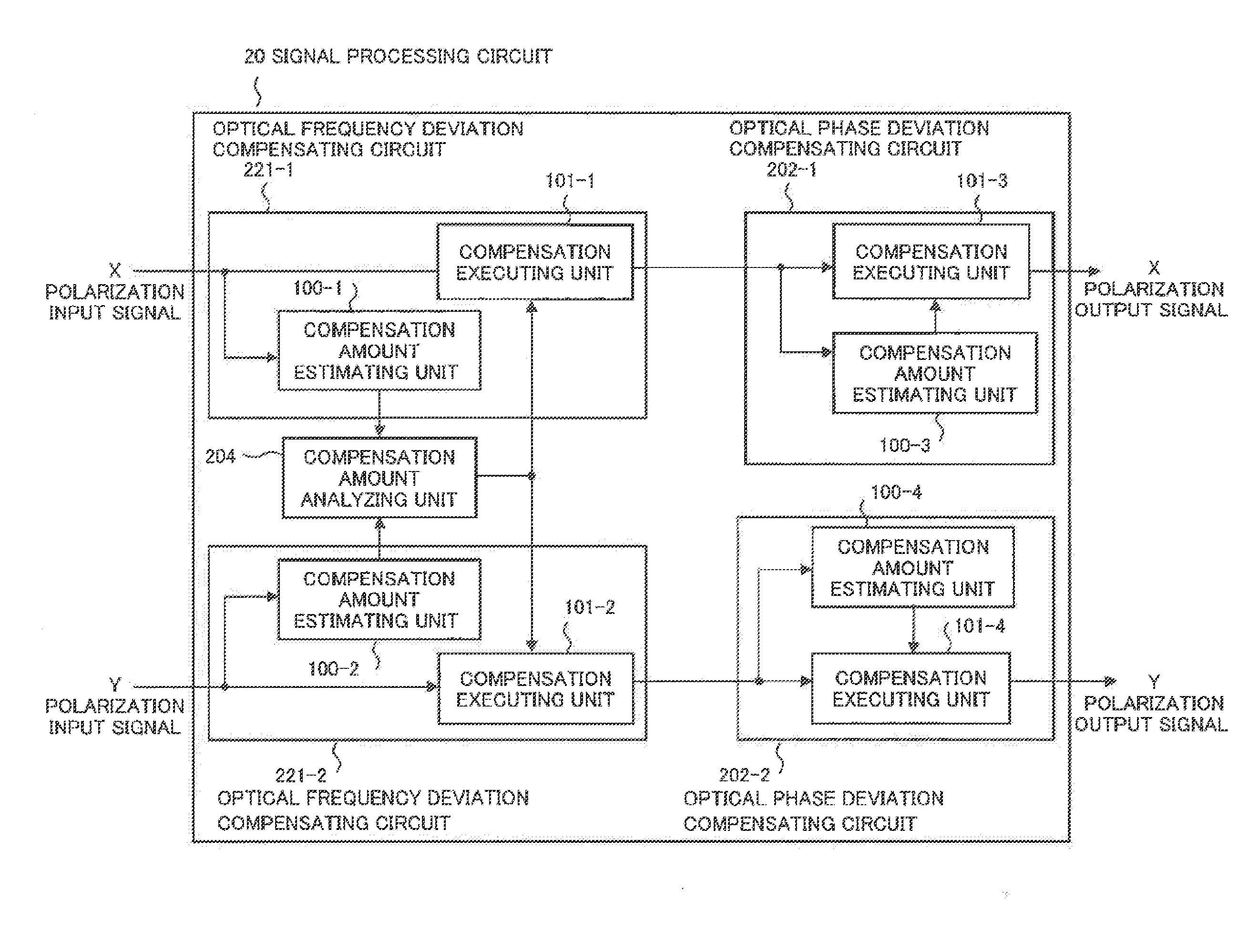
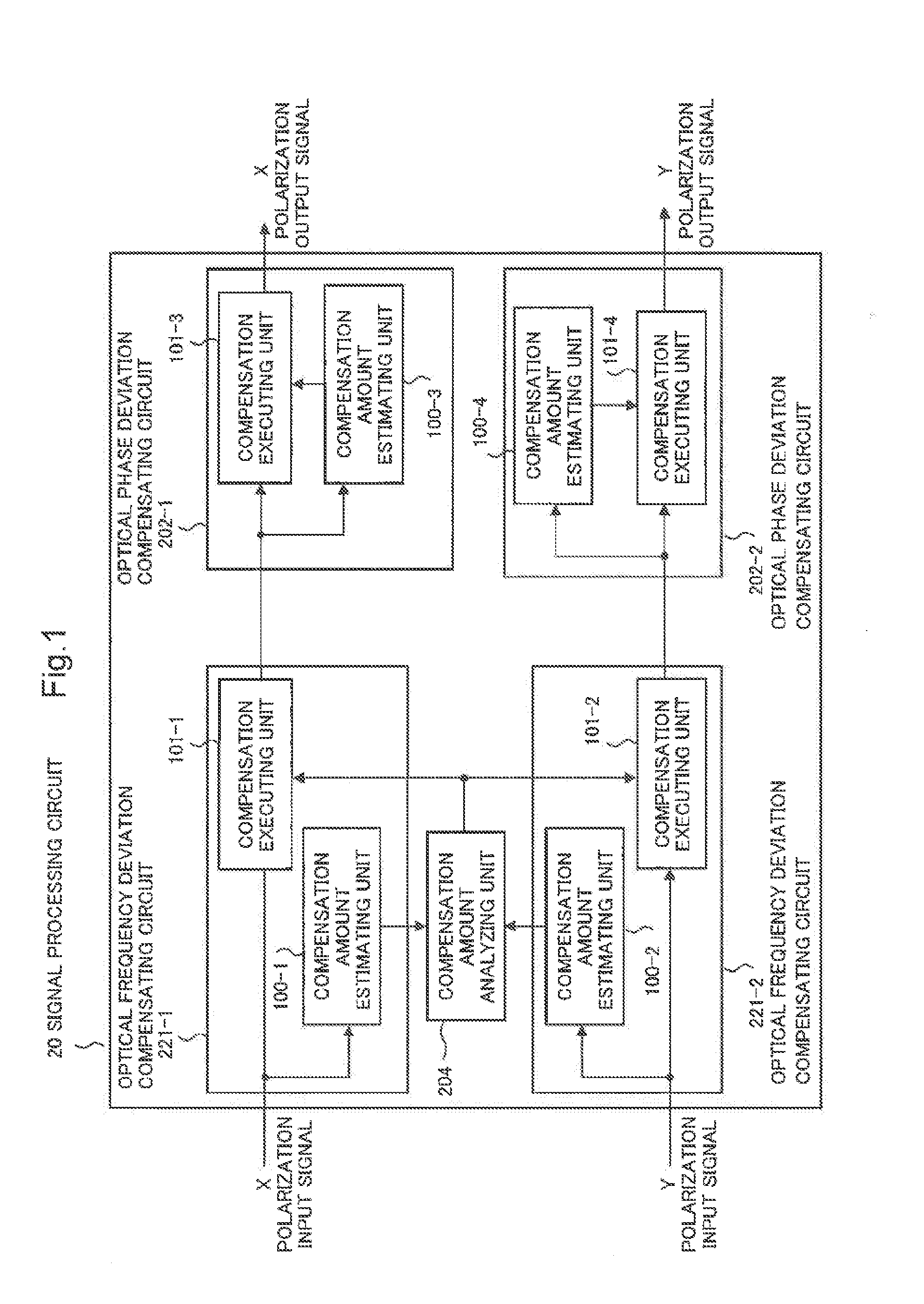
[0054]Hereinafter, a first exemplary embodiment according to the present invention will be described in detail with reference to drawings. Here, the same reference sign as the components shown in FIG. 8 to FIG. 10 is assigned to the components which has the same function of the component shown in FIG. 8 to FIG. 10, and the description of the components may be omitted in some cases.

[0055]FIG. 12 shows a configuration of an optical communication system according to the first exemplary embodiment of the present invention. An optical communication system 500 shown in FIG. 12 includes an optical transmitter 510 and an optical receiver 520.

[0056]The optical transmitter 510 phase-modulates a plurality of optical carrier waves which have polarization planes able to be demultiplexed from each other, by different data respectively and transmits the phase-modulated optical carrier waves. Hereinafter, a configuration that the optical transmitter transmits two optical carrier waves whose polariz...

second exemplary embodiment

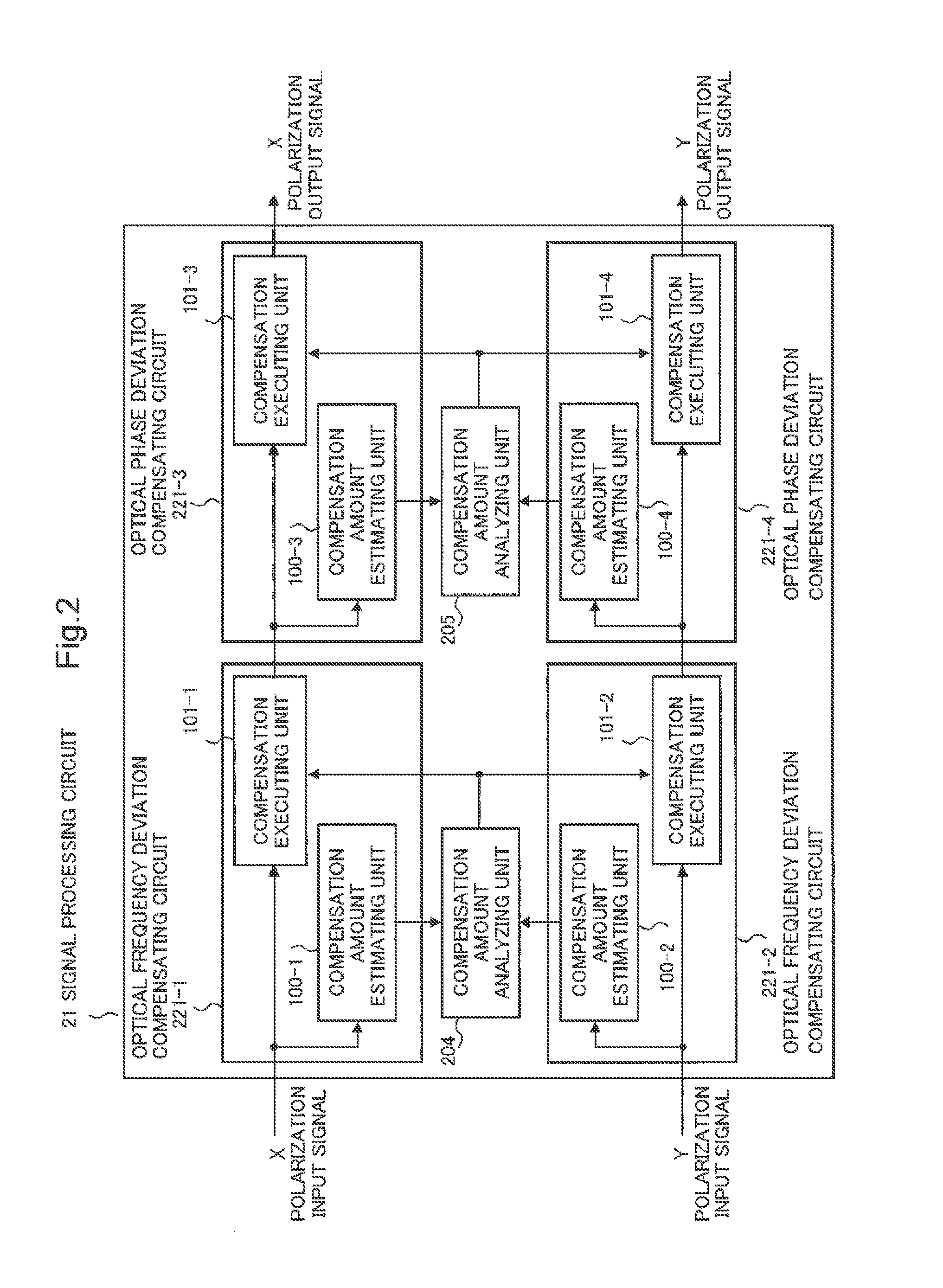
[0091]Next, a signal processing circuit according to a second exemplary embodiment of the present invention will be described.

[0092]The arts described in the patent document 1 and the patent document 2 have a problem that a scale of circuit increases as described below.

[0093]Generally, a clock rate for working LSI is about several hundreds of MHz to 1 GHz. For this reason, it is necessary to arrange circuits in parallel in LSI in order to process a high-speed signal used in the optical communication, for example, a 100 Gbps signal. However, since number of the parallel circuits becomes very large in the case of processing the high speed signal, a circuit scale and electric power consumption of LSI are increased.

[0094]Moreover, in the case of an optical communication system which uses the optical polarization multiplexing / demultiplexing art, number of operations for carrying out the signal processing per an unit time becomes double in comparison with a case of not using the optical p...


PUM


Abstract

In order to reduce influence of noise due to a phase deviation, and to estimate an amount of phase compensation with superior accuracy in a polarization multiplexing / demultiplexing optical communication system, a signal processing circuit includes: optical frequency deviation estimating unit for estimating a frequency deviation which is a difference between a frequency of local light and a frequency of the optical carrier wave which is included in a signal data which corresponds to the polarizations and are generated by mixing a plurality of the optical carrier waves with the local light, which optical carrier wave is phase-modulated and have polarizations able to be demultiplexed and for outputting the estimated frequency deviation as an estimated value; for outputting the estimated frequency deviation as an estimated value; optical frequency deviation compensation amount analyzing unit for calculating an amount of frequency compensation which is an amount of compensation to make a phase of the signal data rotated so as to reduce the frequency deviation, on the basis of a plurality of the estimated values estimated per the signal data; optical frequency deviation compensating unit for making the phase of the signal data rotated correspondingly to the amount of the frequency compensation; optical phase deviation estimating unit for estimating a phase deviation included in each of input signal data and is a difference between a phase of the optical carrier wave and a phase of the local light; and optical phase deviation compensating unit for making the phase of the signal data rotated correspondingly to the phase deviation.

Description

TECHNICAL FIELD[0001]The present invention relates to a signal processing circuit, a signal processing method, an optical receiver and an optical communication system and in particular, relates to an art for compensating an optical phase deviation and an optical frequency deviation of an optical carrier wave in a polarization multiplexing / demultiplexing optical communication system.BACKGROUND ART[0002]As a result of a rapid increase in an amount of traffic of a backbone communication system due to the prevailing Internet, it is desired to develop a practical ultra high speed optical communication system beyond 40 Gbps. As an art which realizes such an ultra high speed optical communication system, the optical phase modulation method and the optical polarization multiplexing / demultiplexing art are noted.[0003]The optical phase modulation method different from the optical intensity modulation method carrying out data modulation of an optical intensity of a laser beam, carries out data...

Claims


Application Information

Patent Timeline
Patent Type & Authority Applications(United States)
IPC IPC(8): H04J14/06H04B10/61
CPCH04B10/614H04B10/6164H04B10/6166H04J14/06H04B10/6162H04B10/6165
Inventor OGASAHARA, DAISAKU
Owner NEC CORP
Why Eureka
Try Eureka