Doped ai paste for local alloyed junction formation with low contact resistance

a technology of low contact resistance and alloyed junctions, which is applied in the field of solar cells, can solve the problems of lowering the conversion efficiency of solar cells, increasing contact resistance, and difficult to get good contact inside the contact openings of alloyed al, so as to reduce the cost-per-watt of solar cells, reduce recombination, and reduce the effect of recombination

US20130255765A1Inactive Publication Date: 2013-10-03APPLIED MATERIALS INC
6 Cites 30 Cited by

Patent Information

Authority / Receiving Office
US · United States
Patent Type
Applications(United States)
Current Assignee / Owner
Publication Date
2013-10-03
Estimated Expiration
Not applicable · inactive patent

Smart Images

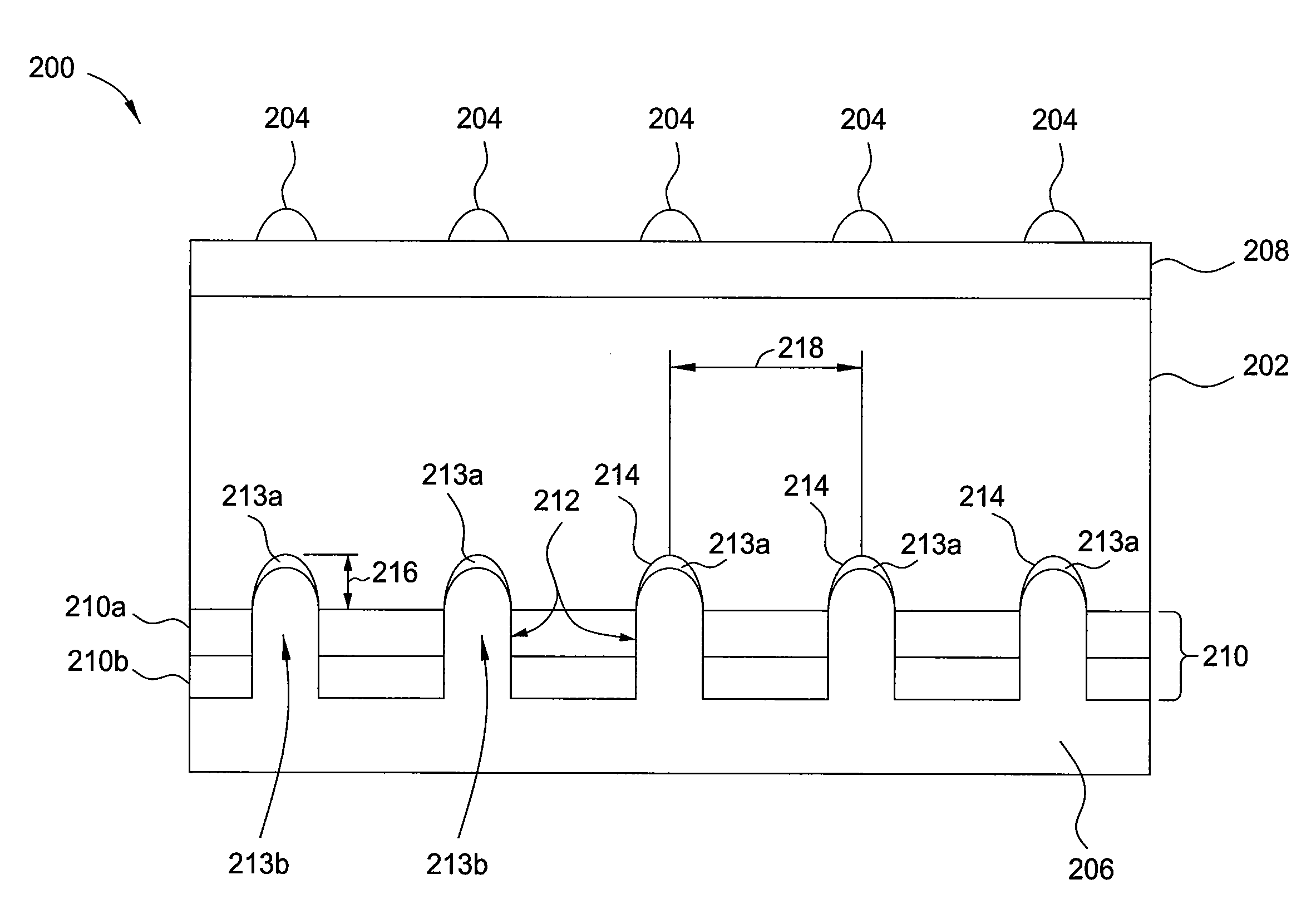
  • Figure 1
    Figure 1
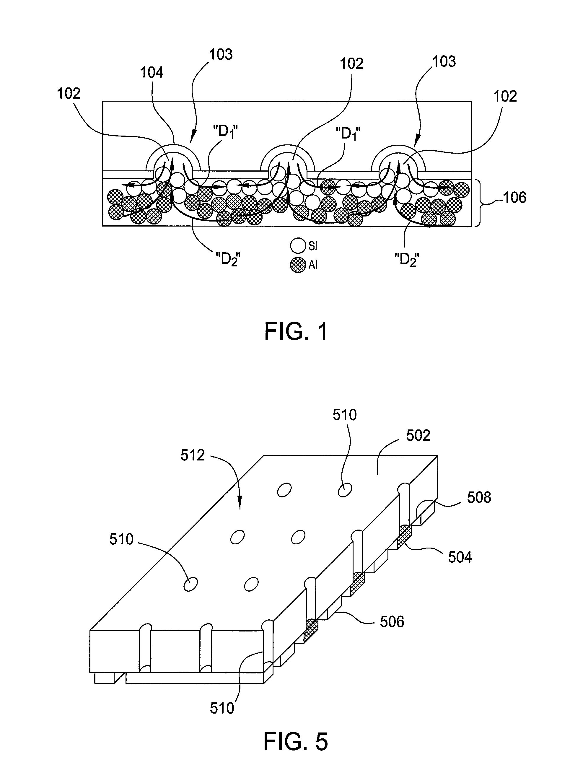
  • Figure 2
    Figure 2
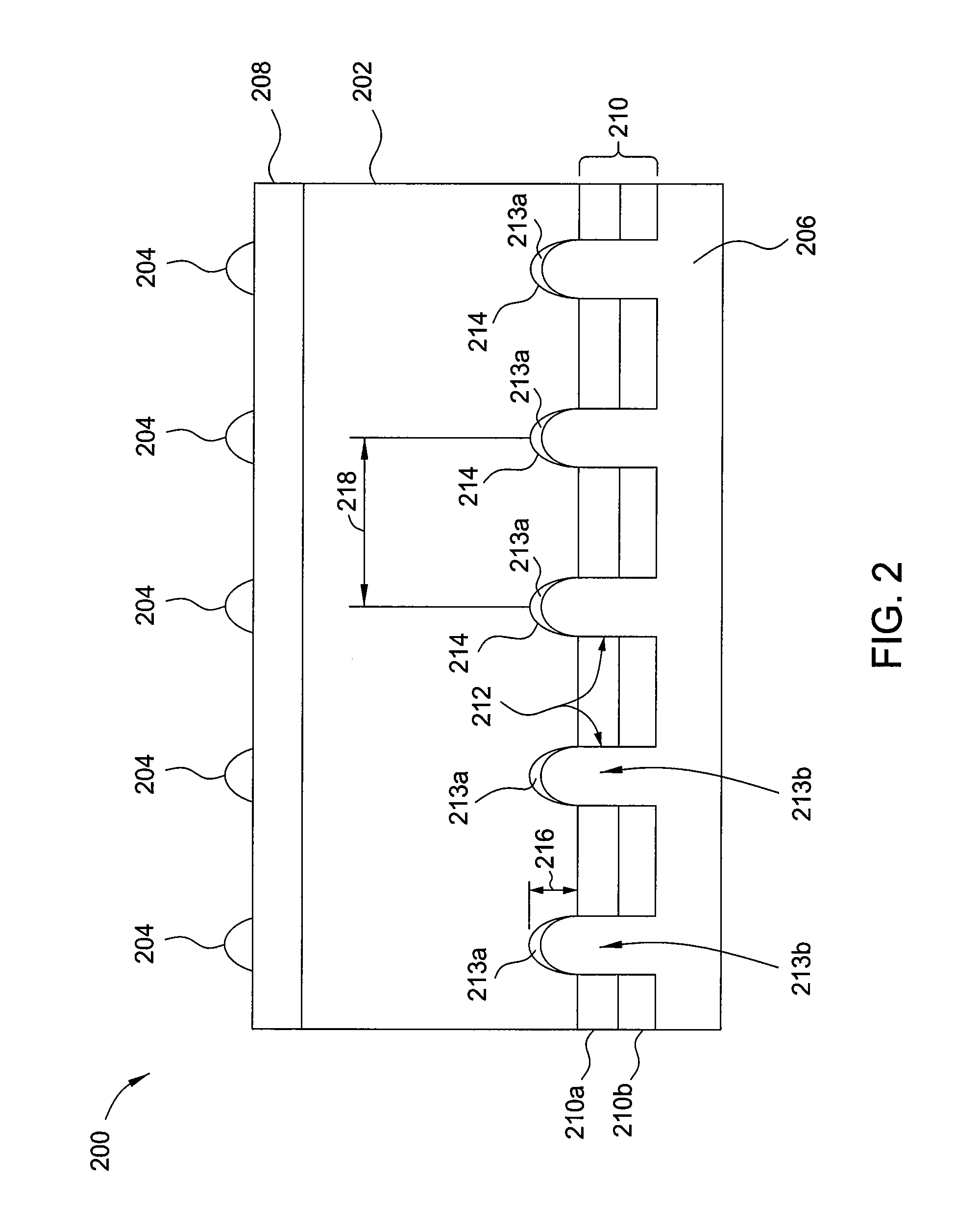
  • Figure 3
    Figure 3
Patent Text Reader

Abstract

Embodiments of the invention generally relate to solar cells having reduced carrier recombination and methods of forming the same. The solar cells have eutectic local contacts and passivation layers which reduce recombination by facilitating formation of a back surface field (BSF). A patterned aluminum back contact doped with a Group III element is disposed on the passivation layer for removing current form the solar cell. The methods of forming the solar cells include depositing a passivation layer including aluminum oxide and silicon nitride on a back surface of a solar cell, and then forming openings through the passivation layer. An aluminum back contact doped with a Group III element is disposed on the passivation layer in a pattern covering the holes, and thermally processed to form a silicon-aluminum eutectic within the openings.
Need to check novelty before this filing date? Find Prior Art

Description

CROSS-REFERENCE TO RELATED APPLICATIONS

[0001] This application claims benefit of U.S. Provisional Patent Application Ser. No. 61 / 618,544, filed Mar. 30, 2012, entitled “DOPED Al PASTE FOR LOCAL ALLOYED JUNCTION FORMATION WITH LOW CONTACT RESISTANCE”, which is herein incorporated by reference.BACKGROUND OF THE INVENTION

[0002] 1. Field of the Invention

[0003] Embodiments of the invention generally relate to solar cells having reduced carrier recombination, and thus higher efficiency, and methods of forming the same.

[0004] 2. Description of the Related Art

[0005] Solar cells generate energy via the photovoltaic effect which is enabled by exposing the solar cells to radiation, such as sunlight. Illumination of a solar cell with radiation creates an electric current as excited electrons and the holes move in different directions through the radiated cell. The electric current may be extracted from the solar cell and used as energy.

[0006] The efficiency of solar cells is directly related to the a...

Examples

Embodiment Construction

[0022]Embodiments of the invention generally relate to methods for manufacturing solar cells. Particularly, embodiments of the invention provide methods of forming a more heavily doped back-surface field (BSF) by forming a metal paste doped with a Group III element on the back surface of the solar cell. The metal paste functions as a back surface contact for the solar cell and may be arranged in grid-like patterns. The grid-like patterned back surface contact reduces the cost-per-watt of the solar cell by using less material than a full-surface back contact. In one embodiment, methods of forming the solar cells include depositing a passivation layer stack including aluminum oxide (AlxOy) and silicon nitride (SixNy) on a back surface of a silicon substrate, and then forming contact openings through the passivation layer stack. A patterned aluminum paste doped with an element, such as boron, is then disposed on the passivation layer stack over the contact openings. Thereafter, the sub...