Thin film capacitor

a film capacitor and capacitor body technology, applied in the direction of capacitors, multiple fixed capacitors, electrical equipment, etc., can solve the problems of complex process, and easy instability of the connection state (electric connection) between the internal electrode layer and the connection electrode, so as to improve the stability of the electric connection and the effect of increasing the connection

Active Publication Date: 2013-10-03
TDK CORPARATION
View PDF3 Cites 33 Cited by
  • Summary
  • Abstract
  • Description
  • Claims
  • Application Information

AI Technical Summary

Benefits of technology

[0008]According to such thin film capacitor, crystal grains of the internal electrode layers are in a range for enabling preferable connection with the connection electrode, and the connection state between the internal electrode layers and the connection electrodes can he stabilized. If the crystal grains of both the internal electrode layers and the connection electrodes are large, the connection state becomes unstable. Based upon this result, it has become possible to improve the stability of the electric connection between the internal electrode layers and the connection electrodes. Then, if the stability of the connection status is improved, effects, such as yield of products becoming excellent, variation of element capacities becoming improved, an increase in ESR enabling restraint and / or reliability becoming improved, can be obtained.
[0009]In the thin film capacitor of the present invention, the exposed internal electrode layers preferably include a protrusion part that protrudes from the dielectric body layer as seen in a lamination direction. It is preferred that the connection electrode is electrically connected to the internal electrode layers via at least a portion of a surface of and an end surface of each of the internal electrode layers, the portion and the end being included in the protrusion part. The protrusion parts can further enlarge the contact areas of both, and can further stabilize the connection status.
[0011]In addition, in the thin film capacitor of the present invention, an under-electrode is preferably Ni foil. If the Ni foil is used for the under-electrode, when a thermal treatment is conducted after the internal electrode layers and the dielectric body layers are laminated and the grain size is controlled, cracks and peeling are hard to occur in the multilayer body, and the crystal grains of the internal electrode layers and the connection electrode can be the most-suitable value. Therefore, the connectivity can be further increased.
[0012]According to the thin film capacitor relating to the present invention, it becomes possible to improve the stability of the electric connection between the internal electrode layers and the connection electrode.

Problems solved by technology

However, it is believed that the configuration of the thin film capacitor described in Patent Literature 1 and Non-Patent Literature 1 where a multilayer structure has been adopted in order to realize larger capacity of the thin film capacitor has the following problems.
However, with this method, not only the process becomes complicated, but only an end surface portion of the internal electrode with very thin film thickness shall be exposed, and because only this end surface portion shall be connected to the connection electrode, the connection state (electric connection) between the internal electrode layers and the connection electrodes easily becomes unstable.
Consequently, there are problems where a capacity of elements varies due to internal electrode layers not being connected, and resistance of the electrodes, i.e., equivalent series resistance (ESR) is increased.
If the crystal grains of both the internal electrode layers and the connection electrodes are large, the connection state becomes unstable.

Method used


Image

  • Thin film capacitor
  • Thin film capacitor
  • Thin film capacitor

Examples


examples

[0046]Hereafter, the present invention is further specifically explained with reference to embodiments. However, the present invention shall not be limited to the embodiments below.

examples 1 to 10

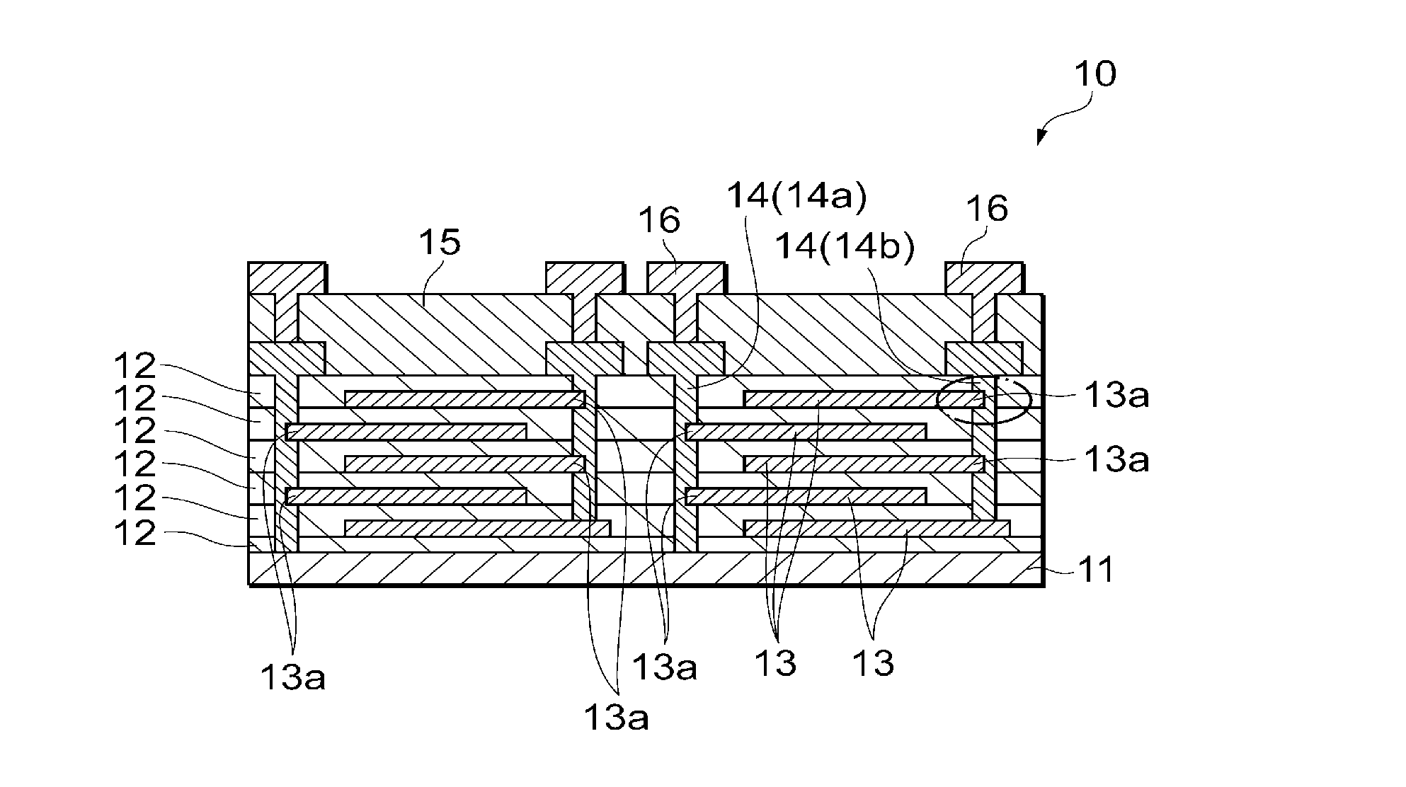
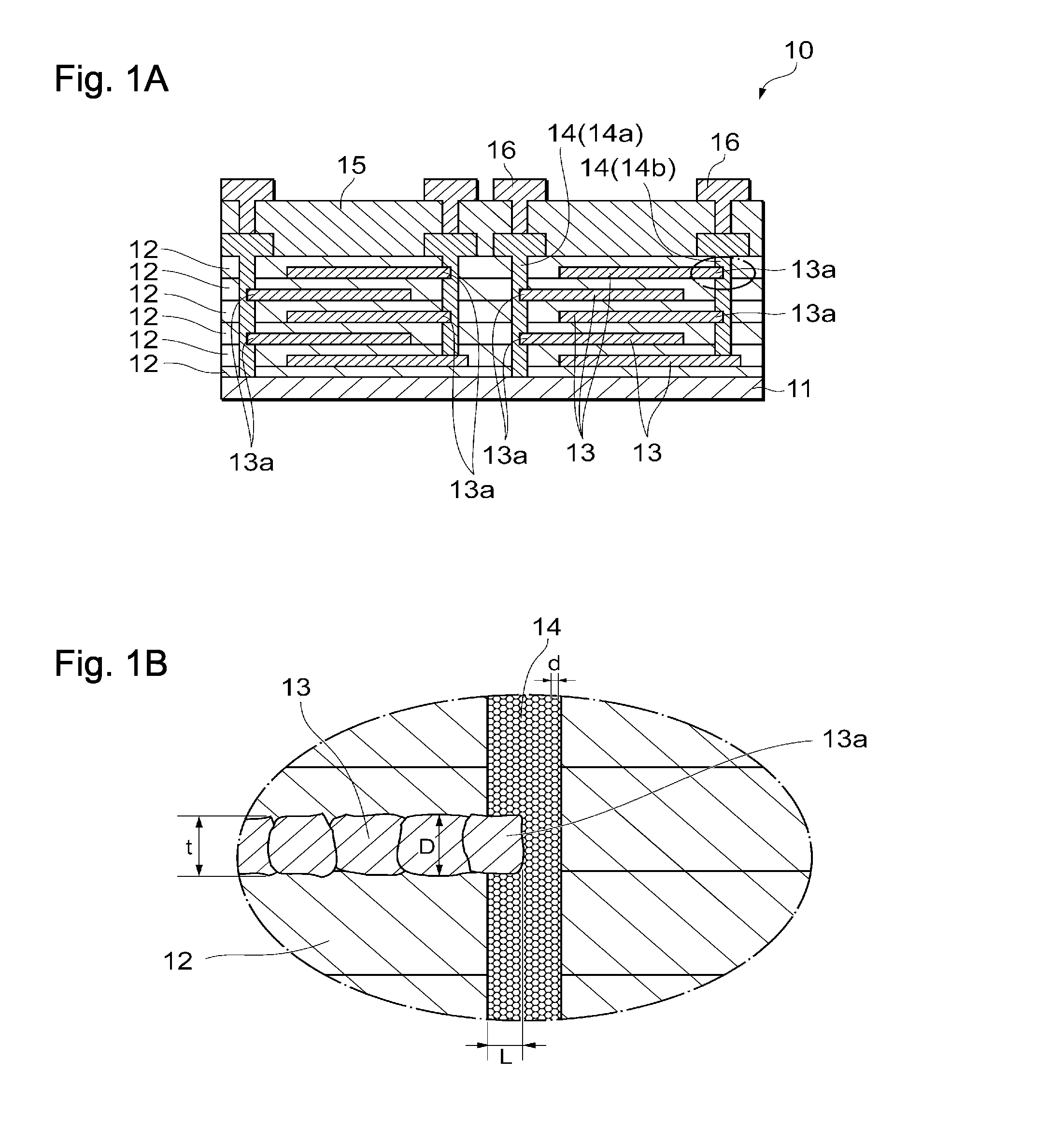
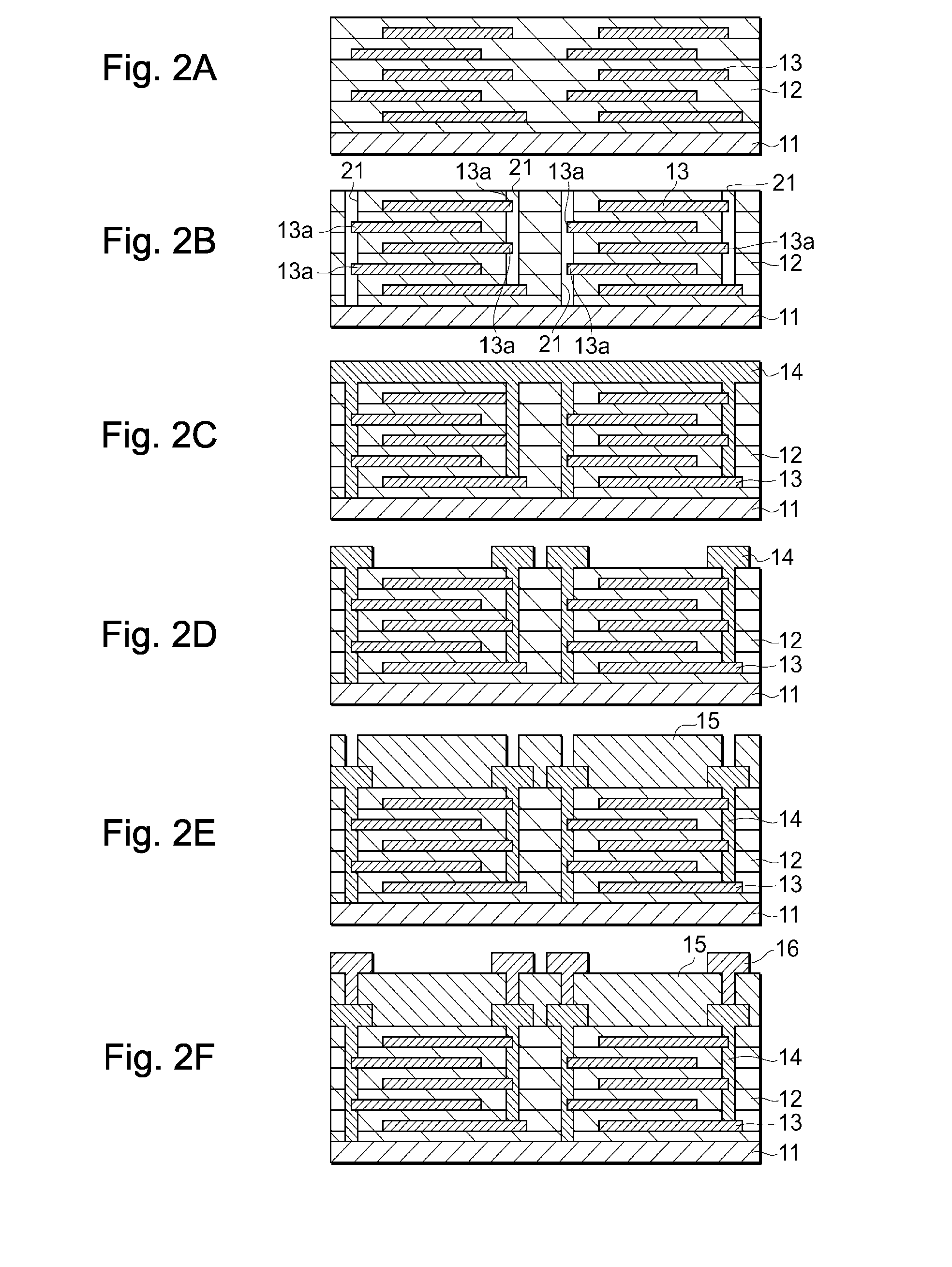
[0047]Thin film capacitors with the similar structure to FIG. 1 were manufactured. The dielectric body layers 12 and the patterned internal electrode layers 13 were alternately laminated onto the Ni foil under-electrode 11 by sputtering. BT was used for the dielectric body layer 12. The thickness of the internal electrode layers was set at 300 nm for Examples 1 to 3, 400 nm for Example 4, 200 rim for Example 5, 100 nm for Example 7, and 500 nm for Examples 8 and 9. Eleven layers of the dielectric body layers 12 were laminated. Due to this, the number of the dielectric body layers 12 sandwiched between the Ni foil under-electrode 11 and the internal electrode layers 13 becomes 10. Electrode shape and dielectric body thickness were set so as to he approximately 5,500 pF (5.5 nF) of one layer of dielectric body layer 12.

[0048]After the dielectric body layers 12 and the internal electrode layers 13 were laminated, a resist layer having the openings 21 was formed on a thermally-treated a...

example 11

[0050]The thin film capacitors 10 were manufactured as similar to Example 3, and the connection conductor layer (connection electrode 14) was made of Ni nanoparticles at the openings of the aggregate. Capacitance and ESR of the capacitors were measured as similar to Example 3, and regarding the capacitance, its mean value and standard deviation were calculated. In addition, the connection conductor layer (connection electrode 14) and the internal electrode layers 13 were cut by FIB, and as similar to the examples above, 10 crystal grain sizes were measured at random. For the measurement, an area of the cross section of one crystal grain was converted to a diameter of circle equivalent, and this was implemented to cross sections of 10 crystal grains at random and an average was obtained, and each was deemed as the average grain size.


PUM

PropertyMeasurementUnit
grain sizeaaaaaaaaaa
average grain sizeaaaaaaaaaa
thicknessaaaaaaaaaa

Abstract

A thin film capacitor includes two or more of dielectric body layers that are alternately laminated on an under-electrode, and internal electrode layers that are laminated between the dielectric body layers, and are exposed off the dielectric body layer, and a connection electrode that is electrically connected to the internal electrode layers via the exposed portion of the internal electrode layers, A relationship between an average grain size D of crystal grains in the internal electrode layers and an average grain size d of crystal grains in the connection electrode is D>d.

Description

TECHNICAL FIELD[0001]The present invention relates to a thin film capacitor.BACKGROUND[0002]For example, like thin film capacitors described in patent and non patent documents below, dielectric body layers and internal electrode layers that are alternately laminated to form a multilayer body constituting multiple layers, and configuration where a portion of this multilayer body is exposed and where a plurality of internal electrode layers are bundled as an electrode are known,PRIOR ART DOCUMENTS[0003]Patent document 1: Japanese Patent Application Laid-Open No. H11-26290[0004]Non patent document 1: CARTS Europe 2006 Proceeding pp 273-280[0005]However, it is believed that the configuration of the thin film capacitor described in Patent Literature 1 and Non-Patent Literature 1 where a multilayer structure has been adopted in order to realize larger capacity of the thin film capacitor has the following problems. In the case of the thin film capacitor, patterning is conducted using techn...

Claims


Application Information

Patent Timeline
Patent Type & Authority Applications(United States)
IPC IPC(8): H01G4/30
CPCH01G4/306H01G4/232H01G4/38H01G4/33
Inventor YANO, YOSHIHIKONAMIKAWA, TATSUOOIKAWA, YASUNOBU
Owner TDK CORPARATION
Why Eureka
Try Eureka