Insensitive dry removal process for semiconductor integration

a technology of semiconductor integration and dry removal process, which is applied in the direction of semiconductor devices, electrical equipment, basic electric elements, etc., can solve the problems of destroying the substrate, requiring delicate and controlled etching techniques, and removing too much non-sacrificial material

Inactive Publication Date: 2013-10-03
APPLIED MATERIALS INC
View PDF22 Cites 174 Cited by
  • Summary
  • Abstract
  • Description
  • Claims
  • Application Information

AI Technical Summary

Benefits of technology

[0005]The present technology provides methods of removing dielectric materials from the surface of a semiconductor substrate that are substantially insensitive to the quality of the material being removed. Sacr

Problems solved by technology

If too much or all of the non-sacrificial material is removed before the sacrificial material is removed, the substrate may be ruined.
Because gate last processing may include sacrificial material removal after non-sacrificial films have been deposited, delicate and controlled etching techniques are needed.
Although a variety of etch techniques are available, few provide removal that accounts both for the type and

Method used


Image

  • Insensitive dry removal process for semiconductor integration
  • Insensitive dry removal process for semiconductor integration
  • Insensitive dry removal process for semiconductor integration

Examples


examples

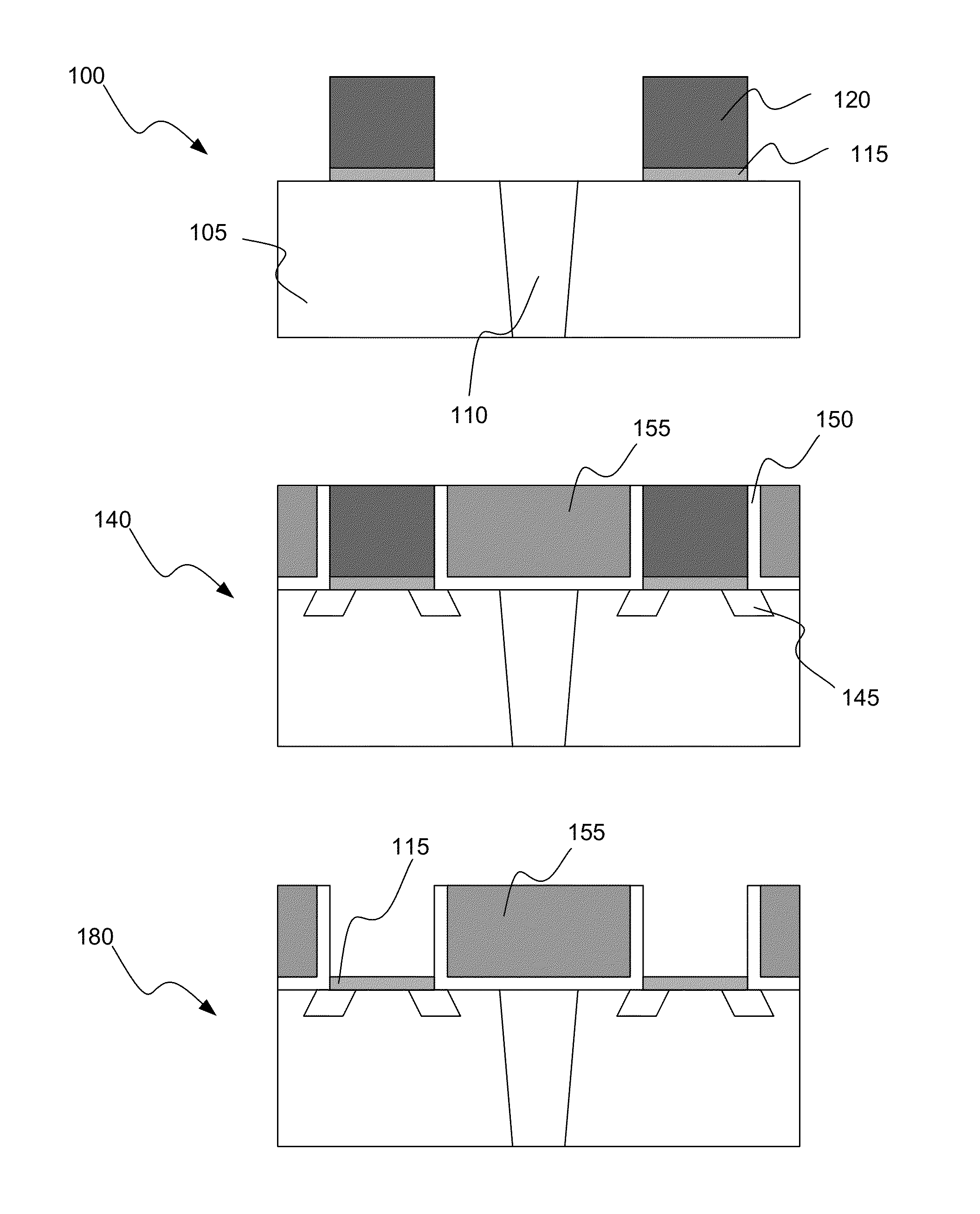
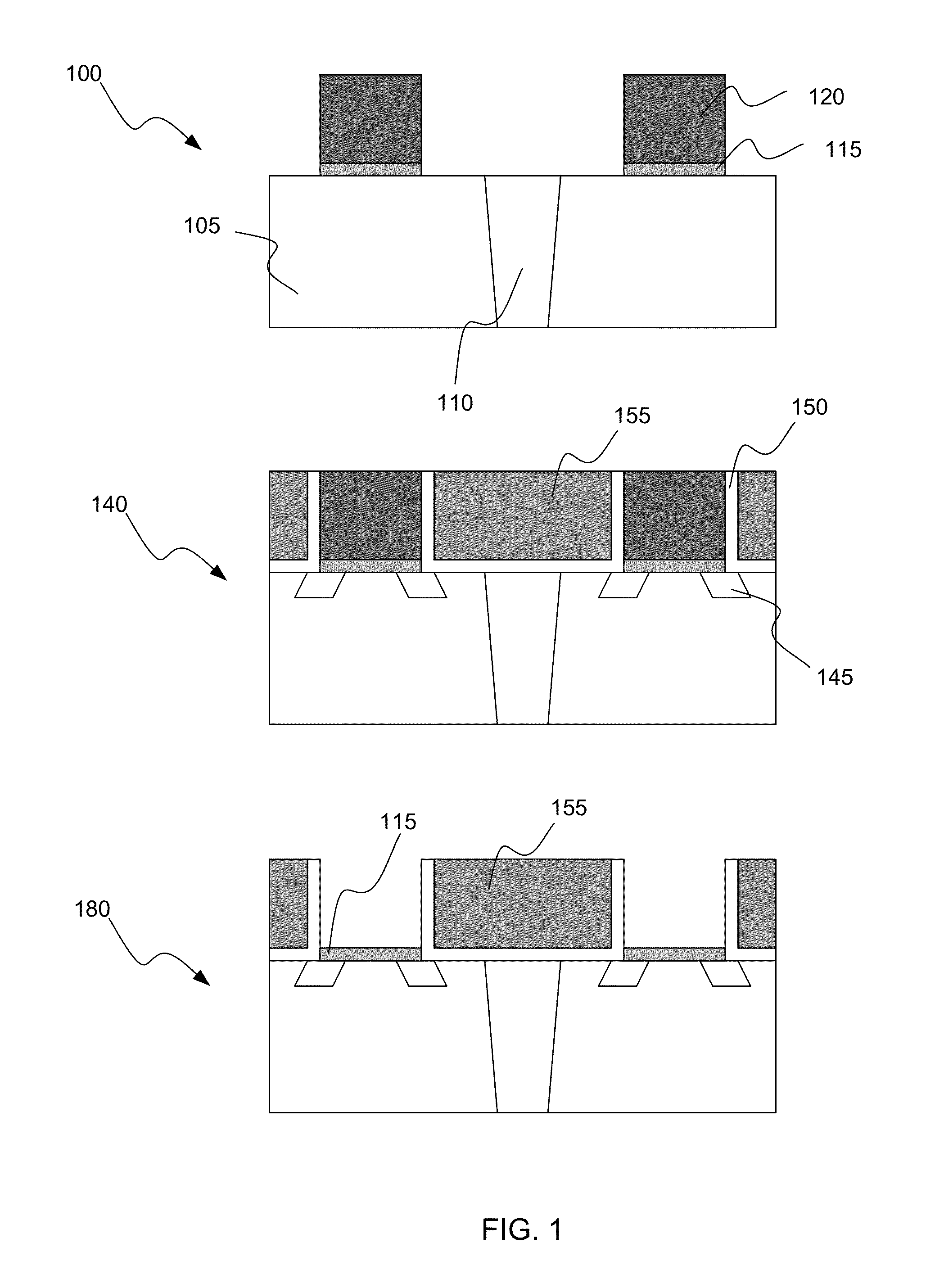
[0046]Comparative examples were made between etch selectivity using a dry etchant gas mixture. The etches were conducted on substrates containing oxides deposited by HDP CVD as well as a flowable CVD. The flowable oxide was cured with an anneal at 400° C. prior to etching. The oxides were exposed to a dry etchant gas mixture containing nitrogen trifluoride and ammonia for a period of thirteen seconds. As can be seen in Table I below, the dry etchant gas mixture removes only slightly more of the flowable oxide as compared to the HDP quality oxide, which indicates that the dry etchant gas is substantially insensitive to oxide quality:

TABLE IETCH DEPTH OF DRY ETCHANT GASEtch DepthSelectivity with(angstrom)respect to HDP oxideHDP Oxide1321.0000Flowable Oxide1331.0076

[0047]FIG. 5A is an SEM image showing etch depth in trenches and open fields using an aqueous HF etchant. The HF is sensitive to oxide quality, and thus differences in oxide quality are reflected in different etch depths. Op...


PUM


Abstract

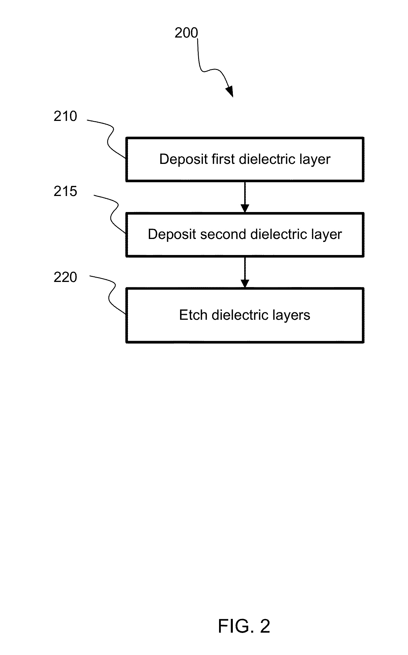
Methods of depositing and etching dielectric layers from a surface of a semiconductor substrate are disclosed. The methods may include depositing a first dielectric layer having a first wet etch rate in aqueous HF. The methods also may include depositing a second dielectric layer that may be initially flowable following deposition, and the second dielectric layer may have a second wet etch rate in aqueous HF that is higher than the first wet etch rate. The methods may further include etching the first and second dielectric layers with an etchant gas mixture, where the first and second dielectric layers have a ratio of etch rates that is closer to one than the ratio of the second wet etch rate to the first wet etch rate in aqueous HF.

Description

CROSS-REFERENCES TO RELATED APPLICATIONS[0001]This application claims the benefit of U.S. Provisional Application No. 61 / 539,270, filed Sep. 26, 2011, entitled “Insensitive Dry Removal Process for Semiconductor Integration.” The entire disclosure of which is incorporated herein.BACKGROUND[0002]Semiconductor processing often includes many distinct manufacturing steps. With the current state of technology, circuit components are routinely formed on nanometer scales, and sensitive manufacturing techniques are required. For instance, in replacement metal gate (“RMG” or “gate last”) processing, a sacrificial material located within a trench or within another feature on a semiconductor substrate may need to be removed in the presence of a non-sacrificial material on the substrate. Etching techniques used to remove the first material may expose both the first and second material to the etchant, which may remove both the sacrificial and non-sacrificial material. If too much or all of the no...

Claims


Application Information

Patent Timeline
IPC IPC(8): H01L29/40
CPCH01L29/401H01L21/31116H01L29/66545H01L29/40114
Inventor SAPRE, KEDARMININNI, ROSSELLATANG, JING
Owner APPLIED MATERIALS INC
Why Eureka
Try Eureka