Display Device and Electronic Device

a technology of electronic devices and display devices, applied in the field of display devices, can solve problems such as strain on viewers, and achieve the effect of reducing the strain on viewers

Active Publication Date: 2013-10-10
SEMICON ENERGY LAB CO LTD
View PDF7 Cites 46 Cited by
  • Summary
  • Abstract
  • Description
  • Claims
  • Application Information

AI Technical Summary

Benefits of technology

[0031]In accordance with the present invention, it is possible to provide a display device that can display

Problems solved by technology

Thus, there has been a problem in that the

Method used


Image

  • Display Device and Electronic Device
  • Display Device and Electronic Device
  • Display Device and Electronic Device

Examples


embodiment 1

[0042]In this embodiment, a configuration of a display device of one embodiment of the present invention and a configuration of a display panel which can be used for the display device of one embodiment of the present invention are described.

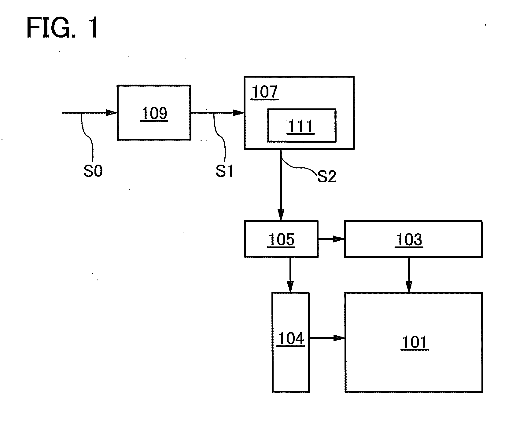
[0043]FIG. 1 is a block diagram illustrating a configuration of a display device according to one embodiment of the present invention. A display device which is exemplified in this embodiment includes a display portion 101, a driver circuit 103, a driver circuit 104, a control circuit 105, an image processing device 107, and a decoder circuit 109.

[0044]The decoder circuit 109 is input with an image signal S0 which is compressed or encoded, decodes the image signal S0, and converts it into a first image signal S1. The first image signal S1 converted here is transmitted to the image processing device 107.

[0045]The image processing device 107 converts the input first image signal S1 into a second image signal S2 containing image data which is prope...

embodiment 2

[0110]In this embodiment, a structure of a display panel which can be used for a display device of one embodiment of the present invention is described.

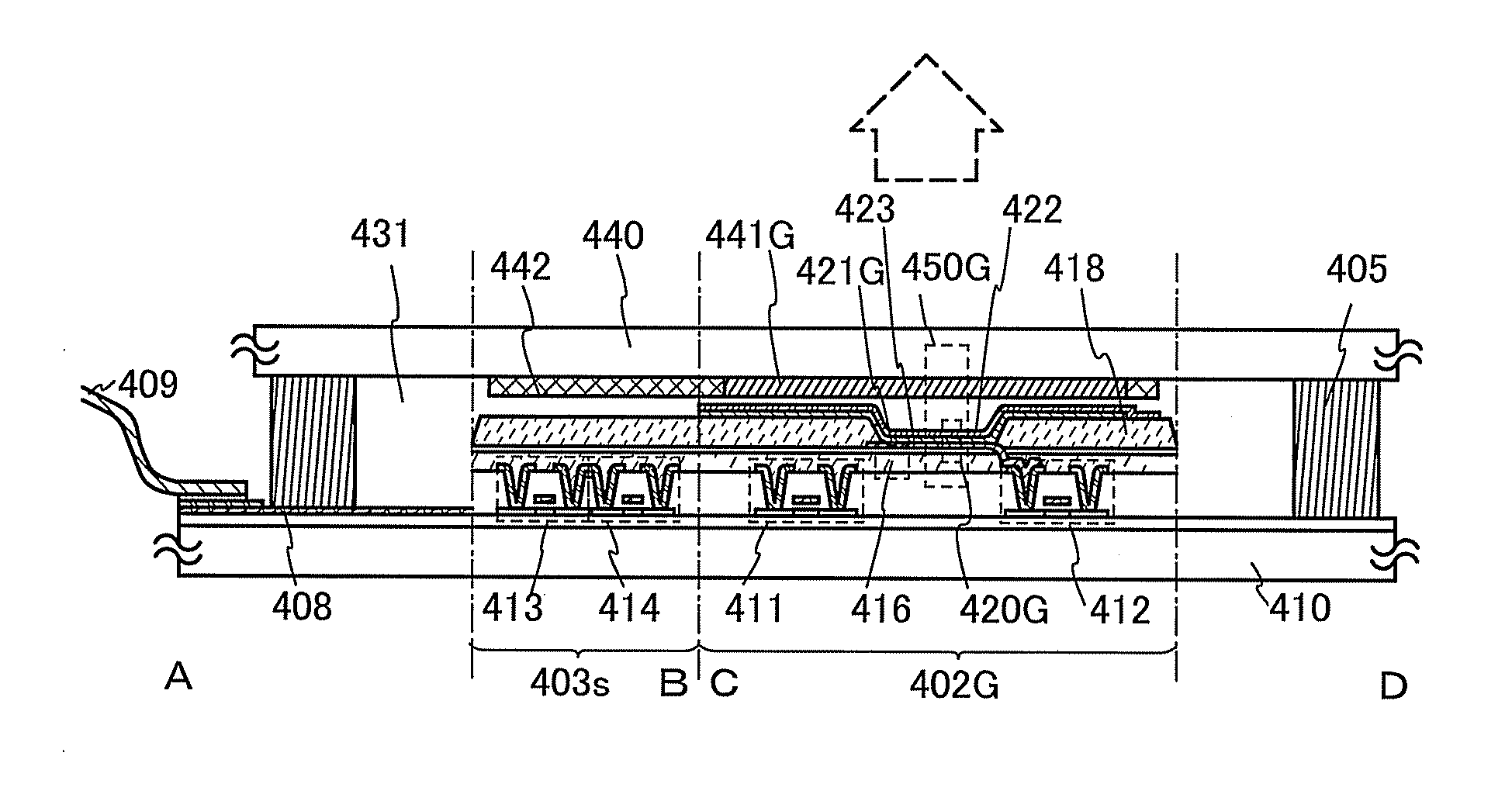
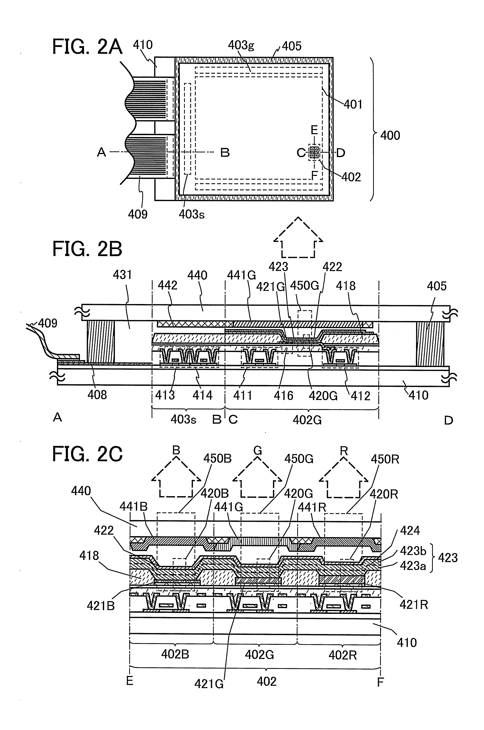
[0111]FIG. 3A is a cross section taken along lines A-B and C-D in FIG. 2A, and FIG. 3B is a cross section taken along lines A-B and C-D in FIG. 2A.

[0112]Although a structure of a top surface of a display panel exemplified in FIG. 3A or FIG. 3B is the same as that of display panel exemplified in Embodiment 1, a structure of a side surface of the display panel exemplified in FIG. 3A or FIG. 3B is different from that of the display panel exemplified in Embodiment 1. Note that portions having the same structure as those described in Embodiment 1 are denoted by the same reference numerals, and the description of Embodiment 1 is applied thereto.

[0113]In the display panel exemplified in FIG. 3A, a display portion including a sub-pixel 402G and a source side driver circuit portion 403s are provided over a first substrate 410. A transistor 47...

embodiment 3

[0143]In this embodiment, the structure of a light-emitting element which can be used for the light-emitting module according to one embodiment of the present invention will be described. Description is given below with reference to FIGS. 4A to 4C.

[0144]The light-emitting element described in this embodiment as an example includes a first electrode, a second electrode, and a layer containing a light-emitting organic compound (hereinafter referred to as an EL layer) provided between the first electrode and the second electrode. Note that one of the first electrode and the second electrode functions as an anode, and the other functions as a cathode. The EL layer is provided between the first electrode and the second electrode, and a structure of the EL layer may be appropriately selected in accordance with materials of the first electrode and second electrode.

[0145]An example of a structure of a light-emitting element is illustrated in FIG. 4A. In the light-emitting element illustrate...


PUM


Abstract

One object of the invention is to provide a display device that can display an image which causes a viewer less strain associated with viewing and gives a viewer a sense of great depth and an electronic device for enjoying the image. The present inventors have focused on a sense of depth obtained by monocular viewing and have conceived a display device in which pixels each include a light-emitting module capable of emitting light having a spectral line half-width of less than or equal to 60 nm in a response time of less than or equal to 100 μs and are provided at a resolution of higher than or equal to 80 ppi; the NTSC ratio is higher than or equal to 80%; and the contrast ratio is higher than or equal to 500.

Description

BACKGROUND OF THE INVENTION[0001]1. Field of the Invention[0002]The present invention relates to a display device. Further, the present invention relates to an electronic device including a display device.[0003]2. Description of the Related Art[0004]A display device that displays a stereoscopic image using a binocular parallax is known. Such a display device is configured to display, on one screen, an image to be seen from the position of the left eye of a viewer (an image for left eye) and an image to be seen from the position of the right eye of the viewer (an image for right eye). The viewer sees the image for left eye with the left eye and the image for right eye with the right eye and is thus allowed to see a stereoscopic image.[0005]For example, in a glasses system, an image for left eye and an image for right eye are alternately displayed on a screen of a display device in synchronization with a shutter provided in a pair of glasses, whereby the left eye of a viewer is allowe...

Claims


Application Information

Patent Timeline
IPC IPC(8): H01L33/50H01L51/52
CPCH01L33/50H01L51/52B82Y20/00H01L27/3244G09G3/003G02F1/13338G09G2300/0426G09G2320/0271G09G2340/0435G09G2360/144G09G3/2003H10K59/12G09F9/00H10K50/80
Inventor YAMAZAKI, SHUNPEIHIRAKATA, YOSHIHARU
Owner SEMICON ENERGY LAB CO LTD
Why Eureka
Try Eureka