Connection Structure

Active Publication Date: 2013-10-17
MURATA MFG CO LTD
View PDF7 Cites 22 Cited by
  • Summary
  • Abstract
  • Description
  • Claims
  • Application Information

AI Technical Summary

Benefits of technology

[0011]Hence, it is an object of the present invention to provide a connection structu

Problems solved by technology

Accordingly, also in this case, the problem that a cr

Method used


Image

  • Connection Structure
  • Connection Structure
  • Connection Structure

Examples


first embodiment

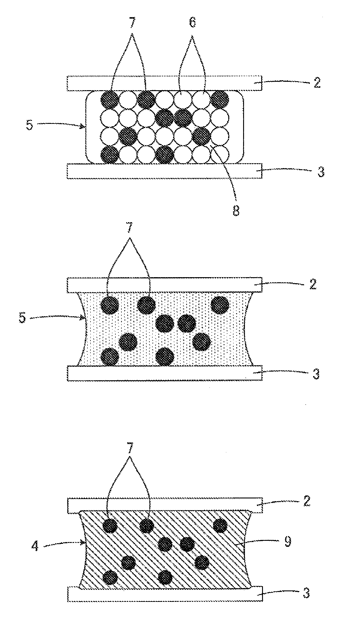
[0030]In reference to FIGS. 1(1) to 1(3), a connection structure 1 according to a first embodiment of the present invention will be described. The connection structure 1 shown in FIG. 1(3) is obtained after undergoing the process from FIG. 1(1) to FIG. 1(2). As shown in FIG. 1(3), the connection structure 1 has a structure in which a first connecting object 2 is connected to a second connecting object 3 with a connecting part 4 interposed therebetween.

[0031]In order to obtain the connection structure 1, first, a solder paste 5 is provided between the first connecting object 2 and the second connecting object 3, as shown in FIG. 1(1). The solder paste 5 includes metal components consisting of a low melting point metal powder 6 of a Sn-based metal and a high melting point metal powder 7 of a Cu-based metal having a higher melting point than that of the Sn-based metal, and a flux 8.

[0032]A Sn-based metal is Sn alone or an alloy containing Sn in an amount of 70% by weight or more, and p...

second embodiment

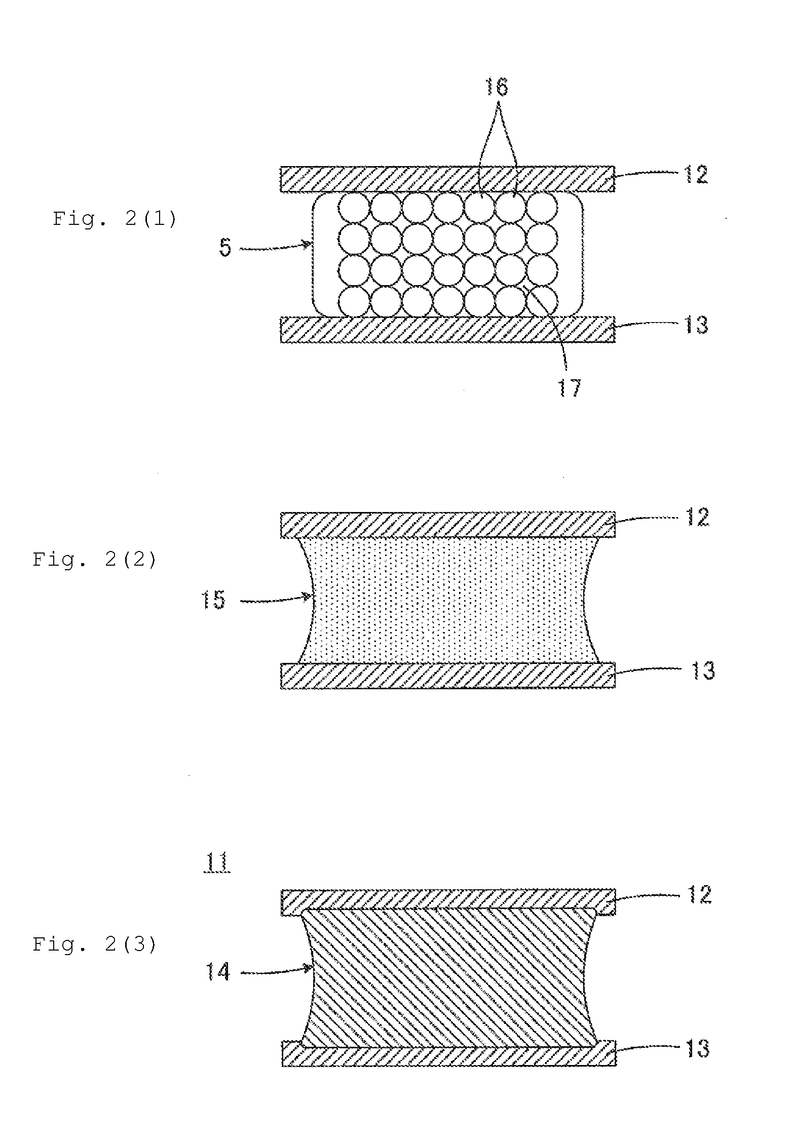
[0061]In reference to FIG. 2, a connection structure 11 according to a second embodiment of the present invention will be described. A connection structure 11 shown in FIG. 2(3) is obtained after undergoing the process from FIG. 2(1) to FIG. 2(2). As shown in FIG. 2(3), the connection structure 11 has a structure in which a first connecting object 12 is connected to a second connecting object 13 with a connecting part 14 interposed therebetween.

[0062]The second embodiment is characterized in that at least surfaces of the first connecting object 12 and the second connecting object 13 are respectively made of a Cu-based metal. In addition, as the Cu-based metal, the same Cu-based metals as those described in the above-mentioned first embodiment can be employed.

[0063]Further, in the second embodiment, a solder paste 15 provided between the first connecting object 12 and the second connecting object 13, shown in FIG. 2(1), includes a low melting point metal powder 16 of a Sn-based metal...

experiment example 1

[0072]In Experiment Example 1, a solder paste was prepared by mixing a low melting point metal powder having a “Sn-based metal component” shown in Table 1, a high melting point metal powder having a “Cu-based Metal Component” shown in Table 1 and a flux.

[0073]The mixing ratio of the Sn-based metal component to the Cu-based metal component was adjusted so as to be 60 / 40 in terms of the volume ratio of the low melting point metal powder to the high melting point metal powder.

[0074]Further, as the flux, a mixture composed of rosin, diethylene glycol monobutyl ether, triethanol amine and hydrogenated castor oil in proportions of 74%:22%:2%:2% by volume was used. The mixing ratio of the flux was adjusted to 10% by weight with respect to the whole solder paste.

[0075]On the other hand, as shown in FIG. 3, a printed board 22 having a Cu land 21 having a size of 0.7 mm×0.4 mm was prepared, and a laminated ceramic capacitor 24 of 1 mm long, 0.5 mm wide and 0.5 mm thick having an external elec...


PUM

PropertyMeasurementUnit
Fractionaaaaaaaaaa
Percent by massaaaaaaaaaa
Percent by volumeaaaaaaaaaa

Abstract

A connection structure that includes a region where at least a Cu—Sn intermetallic compound, a M-Sn intermetallic compound and a Cu-M-Sn intermetallic compound (where M is Ni and/or Mn) exist in a cross-section of a connecting part when the cross-section of the connecting part is analyzed with a WDX. Further, the connection structure is configured so that when the cross-section of the connecting part is evenly divided into ten sections in a vertical direction and a lateral direction, respectively, to form 100 segmentalized squares in total, a ratio of the number of squares in which two or more kinds of intermetallic compounds having different constituent elements exist to the number of all the squares, except for squares in which only a Sn-based metal component exists, is 70% or more.

Description

CROSS REFERENCE TO RELATED APPLICATIONS[0001]The present application is a continuation of International application No. PCT / JP2012 / 052653, filed Feb. 7, 2012, which claims priority to Japanese Patent Application No. 2011-025952, filed Feb. 9, 2011, the entire contents of each of which are incorporated herein by reference.FIELD OF THE INVENTION[0002]The present invention relates to a connection structure in which a first connecting object is connected to a second connecting object with a connecting part interposed therebetween, and to a connection structure that is applied to the case of mounting of electronic parts or via connection, for example, in which a first connecting object is connected to a second connecting object by using a solder as a conductive joining material.BACKGROUND OF THE INVENTION[0003]For example, in the manufacture of electronic equipment including the kind of semiconductor device in which a chip is die bonded or a semiconductor device which is subjected to fli...

Claims


Application Information

Patent Timeline
IPC IPC(8): H01R4/02
CPCH01R4/02B23K35/0244B23K35/025B23K35/262B23K35/302C22C9/02C22C9/05C22C9/06C22C13/00C22C19/03C22C22/00H05K3/3463C22C1/0425H05K2201/0272H05K2201/10636B23K2101/36H05K3/3485Y02P70/50B23K35/26
Inventor NAKANO, KOSUKETAKAOKA, HIDEKIYO
Owner MURATA MFG CO LTD
Why Eureka
Try Eureka