Semiconductor device and manufacturing method thereof

a semiconductor and semiconductor technology, applied in the direction of semiconductor devices, semiconductor/solid-state device details, electrical apparatus, etc., can solve the problems of both the wirings being short-circuited, the damage of the transistor, and the insufficient protection of the semiconductor element such as the transistor provided in the display device from being damaged by esd

Active Publication Date: 2013-10-17
SEMICON ENERGY LAB CO LTD
View PDF14 Cites 28 Cited by
  • Summary
  • Abstract
  • Description
  • Claims
  • Application Information

AI Technical Summary

Benefits of technology

[0020]According to one embodiment of the present invention, a semiconductor device can be provided in which ESD is less likely to occur in a manufacturing process thereof.

Problems solved by technology

However, only the protection circuit formed between the scan electrode of the display device and the conductive line provided in the periphery of the display portion, as described in Patent Document 1, is not sufficient to prevent a semiconductor element such as a transistor provided in the display device from being damaged by ESD.
When the long lead wiring in a floating state (an electrically isolated state) is exposed to a plasma atmosphere, charge is easily accumulated, and ESD is caused by the charge accumulated in the wiring; thus, a transistor might be damaged.
Further, ESD occurs between the wiring and a wiring below the wiring with an insulating layer provided therebetween and the insulating layer is damaged, thus, both the wirings might be short-circuited.

Method used


Image

  • Semiconductor device and manufacturing method thereof
  • Semiconductor device and manufacturing method thereof
  • Semiconductor device and manufacturing method thereof

Examples


embodiment 1

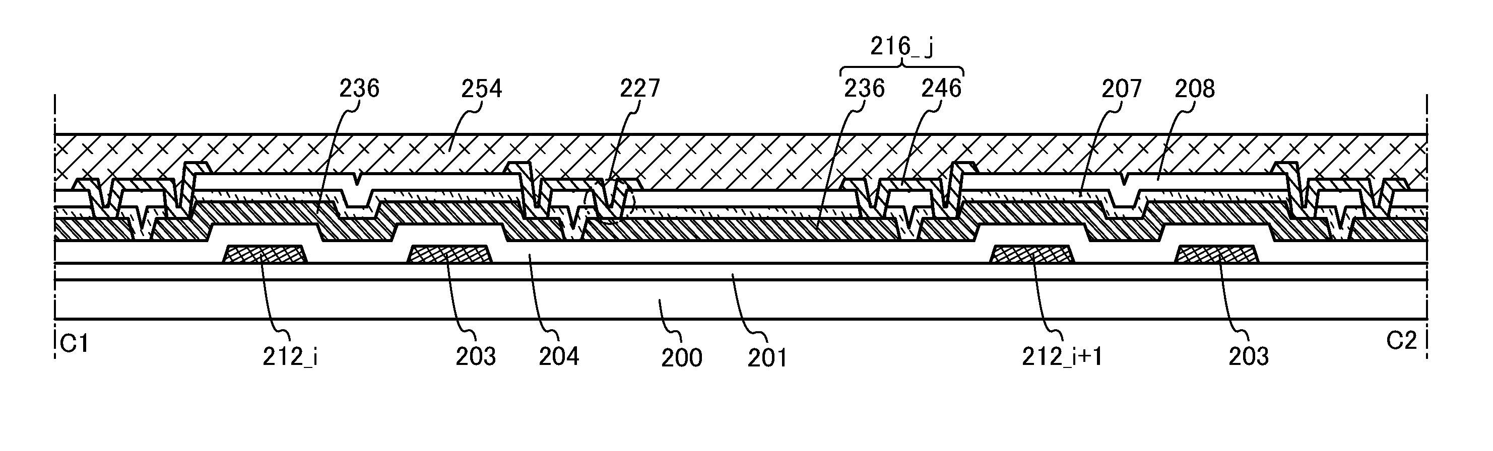
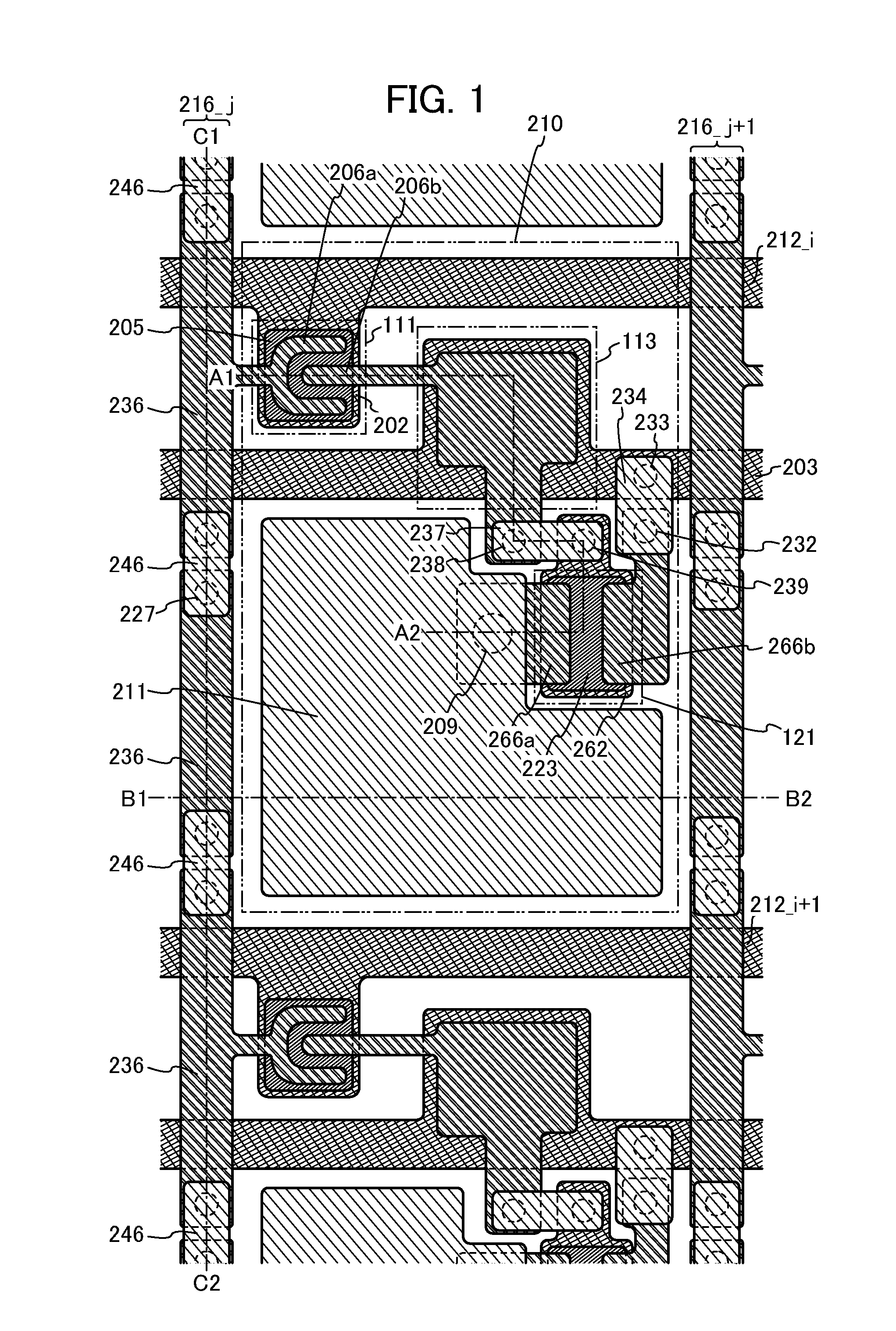
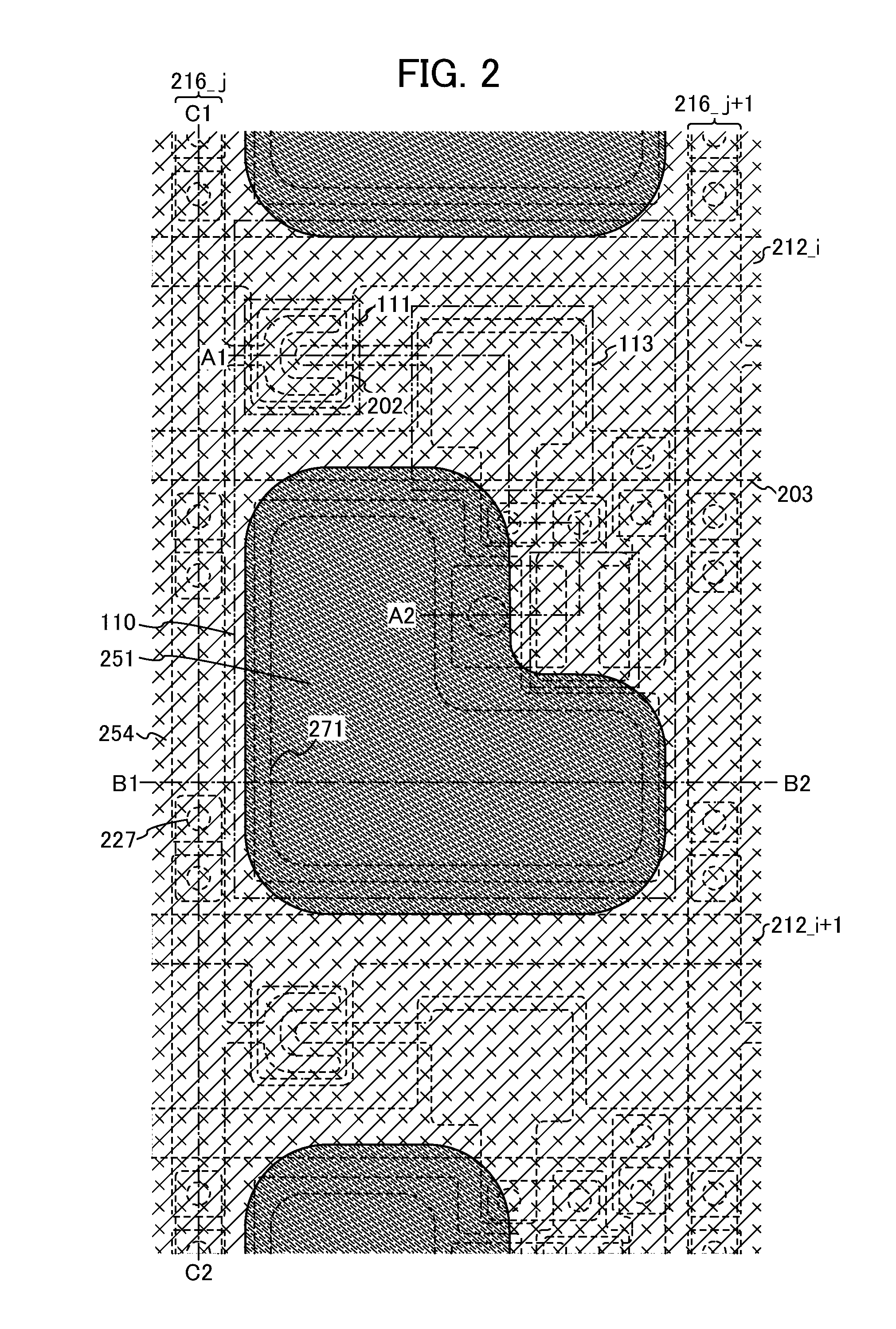
[0052]In this embodiment, examples of a structure of a semiconductor device which is prevented from being damaged by electrostatic discharge or the like are described with reference to FIG. 1, FIG. 2, FIGS. 3A and 3B, FIG. 4, FIGS. 9A to 9C, and FIGS. 10A and 10B. Note that in this embodiment, examples of application thereof to a display device which is an embodiment of a semiconductor device are described.

[0053]FIG. 9A illustrates an example of the circuit configuration of a semiconductor device 100 that is used in a display device. The semiconductor device 100 includes a pixel region 102, a terminal portion 103 including m terminals 105 (m is an integer of greater than or equal to 1) and a terminal 107, and a terminal portion 104 including n terminals 106 (n is an integer of greater than or equal to 1) over a substrate 101. Further, the semiconductor device 100 includes m wirings 212 and a wiring 203 that are electrically connected to the terminal portion 103, and n wirings 216 th...

embodiment 2

[0121]In this embodiment, the wiring 216—j having a structure different from the structure disclosed in Embodiment 1 is described with reference to FIG. 5, FIG. 6, and FIGS. 10A and 10B.

[0122]FIG. 5 is a top view illustrating a plan structure of the pixel 210 and wirings connected to the pixel 210. FIG. 6 is a cross-sectional view of a portion taken along dashed-dotted line D1-D2 in FIG. 5. The wiring 216—j described in this embodiment is different from the wiring 216—j disclosed in Embodiment 1 in the arrangement of the wiring 236. In the wiring 216—j described in this embodiment, the wirings 236 included in the wiring 216—j are formed so as not to overlap with a wiring below the wirings 236. Specifically, the wirings 236 are formed so as not to overlap with the wiring 212—i and the wiring 203. FIG. 10B is an equivalent circuit diagram of the wiring 216—j described in this embodiment.

[0123]The plurality of island-shaped wirings 236 is formed for the long lead wiring 216—j during st...

embodiment 3

[0126]In this embodiment, the wiring 216—j having a structure different from the structures disclosed in Embodiments 1 and 2 is described with reference to FIG. 7 and FIG. 8.

[0127]FIG. 7 is a top view illustrating a plan structure of the pixel 210 and wirings connected to the pixel 210. FIG. 8 is a cross-sectional view of a portion taken along dashed-dotted line E1-E2 in FIG. 6. The wiring 216—j described in this embodiment is different from the wirings 216—j disclosed in Embodiments 1 and 2 in that part of the plurality of wirings 236 included in the wiring 216—j disclosed in Embodiment 2 is a wiring 226 formed using the same conductive layer as the wiring 212—i. FIG. 11 is an equivalent circuit diagram of the wiring 216—j described in this embodiment.

[0128]In the case where the wiring 212—i is formed using a conductive layer containing a material having low resistivity, such as Cu, part of the wiring 216—j is the wiring 226 formed using the same conductive layer as the wiring 212—...


PUM


Abstract

A semiconductor device is provided in which ESD is less likely to occur in a manufacturing process thereof. In manufacture of a semiconductor device including a long lead wiring A, during steps with direct exposure to a plasma atmosphere, a plurality of island-shaped wirings is formed for the wiring A and then electrically connected to one another in series. Specifically, a plurality of island-shaped wirings is formed, covered with an insulating layer, and electrically connected to one another in series by a wiring formed over the insulating layer. The island-shaped wiring and the wiring formed over the insulating layer are electrically connected to each other through an opening formed in the insulating layer.

Description

BACKGROUND OF THE INVENTION[0001]1. Field of the Invention[0002]The present invention relates to a semiconductor device in which ESD is less likely to occur in a manufacturing process and a manufacturing method thereof.[0003]In this specification and the like, the semiconductor device refers to any device which can function by utilizing semiconductor characteristics; an electro-optical device, a display device, a semiconductor circuit, and an electronic device are all included in the category of the semiconductor device.[0004]2. Description of the Related Art[0005]In a semiconductor circuit used in a semiconductor device such as a display device, a semiconductor element, an electrode, an insulating layer, or the like could be damaged by electrostatic discharge (hereinafter referred to as “ESD”). As a measure to prevent damage of a semiconductor circuit due to ESD, a protection circuit is connected to a semiconductor circuit in many cases. A protection circuit refers to a circuit for...

Claims


Application Information

Patent Timeline
Patent Type & Authority Applications(United States)
IPC IPC(8): H01L29/786H01L29/66H01L23/52
CPCH01L29/786H01L23/52H01L29/66477H01L23/60H01L27/1225H01L27/124H01L2924/0002H01L2924/00H01L27/04H01L27/0248H01L27/1244
Inventor YAMAZAKI, SHUNPEI
Owner SEMICON ENERGY LAB CO LTD
Why Eureka
Try Eureka