Semiconductor device

a semiconductor device and semiconductor technology, applied in the direction of semiconductor devices, basic electric elements, electrical equipment, etc., can solve problems such as disconnection, and achieve the effects of reducing the off-state current of the semiconductor device, preventing degradation of electrical characteristics, and favorable electrical characteristics

Inactive Publication Date: 2013-10-17
SEMICON ENERGY LAB CO LTD
View PDF11 Cites 9 Cited by
  • Summary
  • Abstract
  • Description
  • Claims
  • Application Information

AI Technical Summary

Benefits of technology

[0030]However, to reduce the off-state current of the semiconductor device, the low-resistance regions including a dopant are not necessarily provided in the oxide semiconductor film.
[0031]According to one embodiment of the present invention, in a top-gate semiconductor device in which a source electrode and a drain electrode are provided in contact with an oxide semiconductor film, a sidewall insulating film is provided to fill a recessed portion between the source electrode and a gate electrode and a recessed portion between the drain electrode and the gate electrode and to cover part of the source electrode and part of the drain electrode, whereby the step coverage with a film to be formed over the gate electrode, the source electrode, and the drain electrode can be improved. Therefore, an insulating film which is capable of preventing degradation of the electrical characteristics can be provided without a defect such as a disconnection, so that a semiconductor device with favorable electrical characteristics and high performance can be provided.
[0032]According to one embodiment of the present invention, a defect in the manufacturing process, such as a disconnection, can be prevented, so that a semiconductor device can be provided with a high yield and high productivity.
[0033]Further, according to one embodiment of the present invention, on-state current can be increased by providing a low-resistance region containing a dopant in an oxide semiconductor film, so that a semiconductor device with favorable electrical characteristics and high performance can be provided.

Problems solved by technology

However, when the aspect ratio of the gate electrode of the transistor is high, there is a possibility that disconnection occurs in a film which is formed over the gate electrode by a sputtering method or the like which provides low step coverage.

Method used


Image

  • Semiconductor device
  • Semiconductor device
  • Semiconductor device

Examples


embodiment 1

[0064]In this embodiment, a semiconductor device of one embodiment of the present invention will be described with reference to drawings.

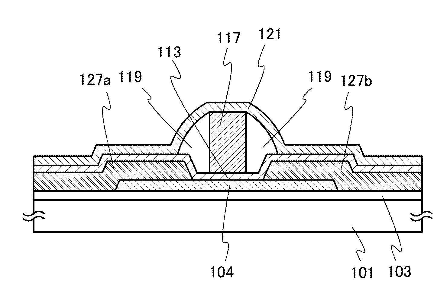
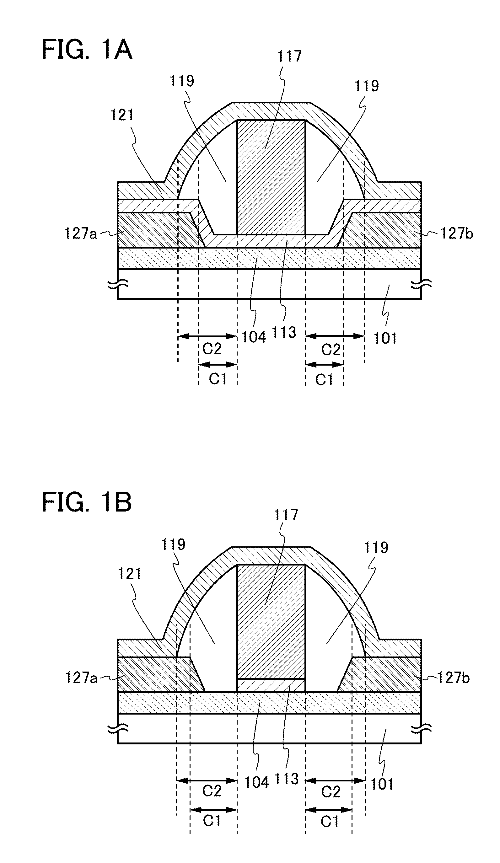
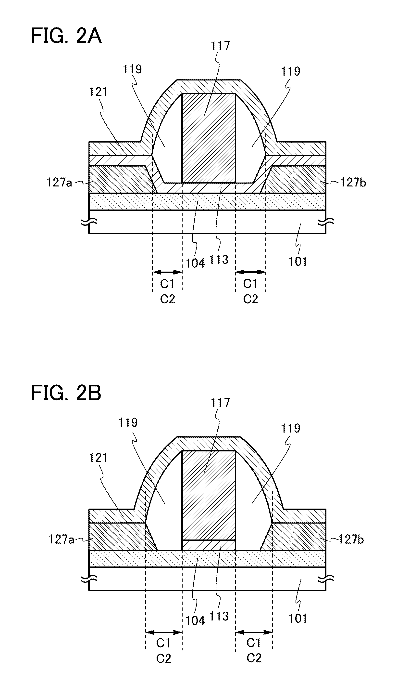
[0065]FIGS. 1A and 1B are cross-sectional views each illustrating a transistor which is one embodiment of the present invention.

[0066]Each of the transistors illustrated in FIGS. 1A and 1B is a top-gate transistor and includes at least an oxide semiconductor film 104, a gate insulating film 113, a gate electrode 117, a source electrode 127a, a drain electrode 127b, a sidewall insulating film 119, and an insulating film 121, over a substrate 101. Note that a base insulating film may be provided between the substrate 101 and the oxide semiconductor film 104, and an interlayer insulating film may be provided over the insulating film 121.

[0067]The transistor illustrated in FIG. 1A has a structure in which the gate insulating film 113 is provided between the sidewall insulating film 119 and each of the source electrode 127a and the drain electrode 127b....

embodiment 2

[0215]In this embodiment, a semiconductor device having a structure which is partly different from that of the semiconductor device described in the above embodiment will be described. Also in this embodiment described below, a transistor is described as a semiconductor device. In this embodiment described below, the drawings (including reference numerals and hatching patterns) and descriptions in the above embodiment are used as appropriate, and points described in the above embodiment are not repeated in some cases.

[0216]A transistor 200 described in this embodiment is different from the transistor 100 described in Embodiment 1 in that an oxide semiconductor film includes a first region functioning as a channel formation region, a pair of second regions between which the first region is provided, and a pair of third regions between which the first region and the pair of second regions are provided.

[0217]The first region, the pair of second regions, and the pair of third regions ca...

embodiment 3

[0240]In this embodiment, a semiconductor device having a structure which is partly different from that of the semiconductor device described in the above embodiment will be described.

[0241]A transistor 300 described in this embodiment is different from the transistor 100 described in Embodiment 1 in that an oxide semiconductor film includes a first region which does not contain a dopant and functions as a channel formation region, a pair of second regions which contain a dopant and between which the first region is provided, and a pair of third regions which contain a dopant and between which the first region and the pair of second regions are provided.

[0242]The first region, the pair of second regions, and the pair of third regions can be formed in a self-aligned manner by injection of a dopant through the gate insulating film, the source electrode, and the drain electrode with the use of the gate electrode as a mask.

[0243]FIGS. 9A and 9B are a top view and a cross-sectional view ...


PUM


Abstract

A semiconductor device preventing a defect in manufacturing process, such as disconnection of a film to be formed. Further, a semiconductor device with favorable electric characteristics and high performance can be provided. In a top-gate semiconductor device in which a source electrode and a drain electrode are provided in contact with an oxide semiconductor film, a sidewall insulating film is provided to fill a recessed portion between the source electrode and a gate electrode and a recessed portion between the drain electrode and the gate electrode, which cause disconnection of a film to be formed on and in contact with the gate electrode. Further, the sidewall insulating film is provided so that a recessed portion is not formed between the sidewall insulating film and another film included in the semiconductor device.

Description

BACKGROUND OF THE INVENTION[0001]1. Field of the Invention[0002]The invention disclosed relates to a semiconductor device.[0003]Note that a semiconductor device in this specification refers to general devices which can function by utilizing semiconductor characteristics; for example, a semiconductor element such as a transistor, a semiconductor circuit including a semiconductor element, an electro-optical device such as a display device, and an electronic device are all semiconductor devices.[0004]2. Description of the Related Art[0005]Transistors used for most flat panel displays typified by a liquid crystal display device and a light-emitting display device are formed using silicon semiconductors such as amorphous silicon, single crystal silicon, and polycrystalline silicon provided over glass substrates. Further, transistors formed using such silicon semiconductors are used in integrated circuits (ICs) and the like.[0006]In recent years, attention has been drawn to a technique in...

Claims


Application Information

Patent Timeline
Patent Type & Authority Applications(United States)
IPC IPC(8): H01L29/78
CPCH01L29/78H01L29/7869H01L27/1225H10B41/70
Inventor YAMAZAKI, SHUNPEI
Owner SEMICON ENERGY LAB CO LTD
Why Eureka
Try Eureka