Eureka AIR delivers breakthrough ideas for toughest innovation challenges, trusted by R&D personnel around the world.

Adaptive resistive device and methods thereof

Active Publication Date: 2013-10-24
THE BOARD OF TRUSTEES OF THE UNIV OF ILLINOIS
View PDF3 Cites 10 Cited by
  • Summary
  • Abstract
  • Description
  • Claims
  • Application Information

AI Technical Summary

Benefits of technology

The patent text describes an invention of a new type of memory device that can store data using a phase change material with carbon nanotubes and graphene electrodes. The device has several advantages over traditional memory devices, including being faster, more robust, and more power-efficient. The technical effects of this invention include the ability to achieve low-power terabyte storage through a universal memory that is immune to the limitations of current memory technologies. The invention also addresses the need for a non-volatile memory that can retain data even when power is turned off. The patent text describes the process of creating the device and conducting experiments to demonstrate its functionality.

Problems solved by technology

Hard drives contain movable parts and are slower, less robust, and more power-hungry than solid-state memory.
However, a need for radiation hardness and non-volatility (retain memory state when power is off) make electrical charge storage like Flash unfeasible at the smallest scales, when a bit consists of only a hundred (or fewer) electrons, such as below a 35 nm technology node.
Such few stored electrons lead to significant statistical bit-to-bit variation, as well as poor charge retention, since long-term storage imposes drastic leakage current limits, of the order of one or two electrons per month.
Another drawback of Flash is its high write / erase voltage (˜15 V), which is needed for tunneling in / out of the floating gate.
Such voltages are incompatible with the low 1-2 V used in logic operation, and large-area charge pumps are often used for the step-up, consuming valuable on-chip real estate.
Phase change materials (PCMs) are promising candidates for nonvolatile data storage and reconfigurable electronics, but high programming currents have presented a challenge to realize low power operation.
However, a drawback of PCM state-of-the-art storage prior to this work has been the high programming current (>0.1 mA), as Joule heat must be coupled to a finite bit volume, previously achieved with 30 to 100-nm diameter nanowires (9-11) or metal vias (12-14).
Of course, while the CNT breakdown method is extremely useful here, it would not be the preferred route for obtaining nanogaps in a more scalable manufacturing environment.
There, the CNT break in vacuum could lead to SiO2 damage, which was not seen here either in ambient air or under Ar flow.
Such record-low power is achieved because of the extremely low effective bit volumes (hundreds of cubic nanometers) that can be addressed with CNT electrodes of few-nanometer diameters.

Method used


Image

  • Adaptive resistive device and methods thereof
  • Adaptive resistive device and methods thereof
  • Adaptive resistive device and methods thereof

Examples


Embodiment Construction

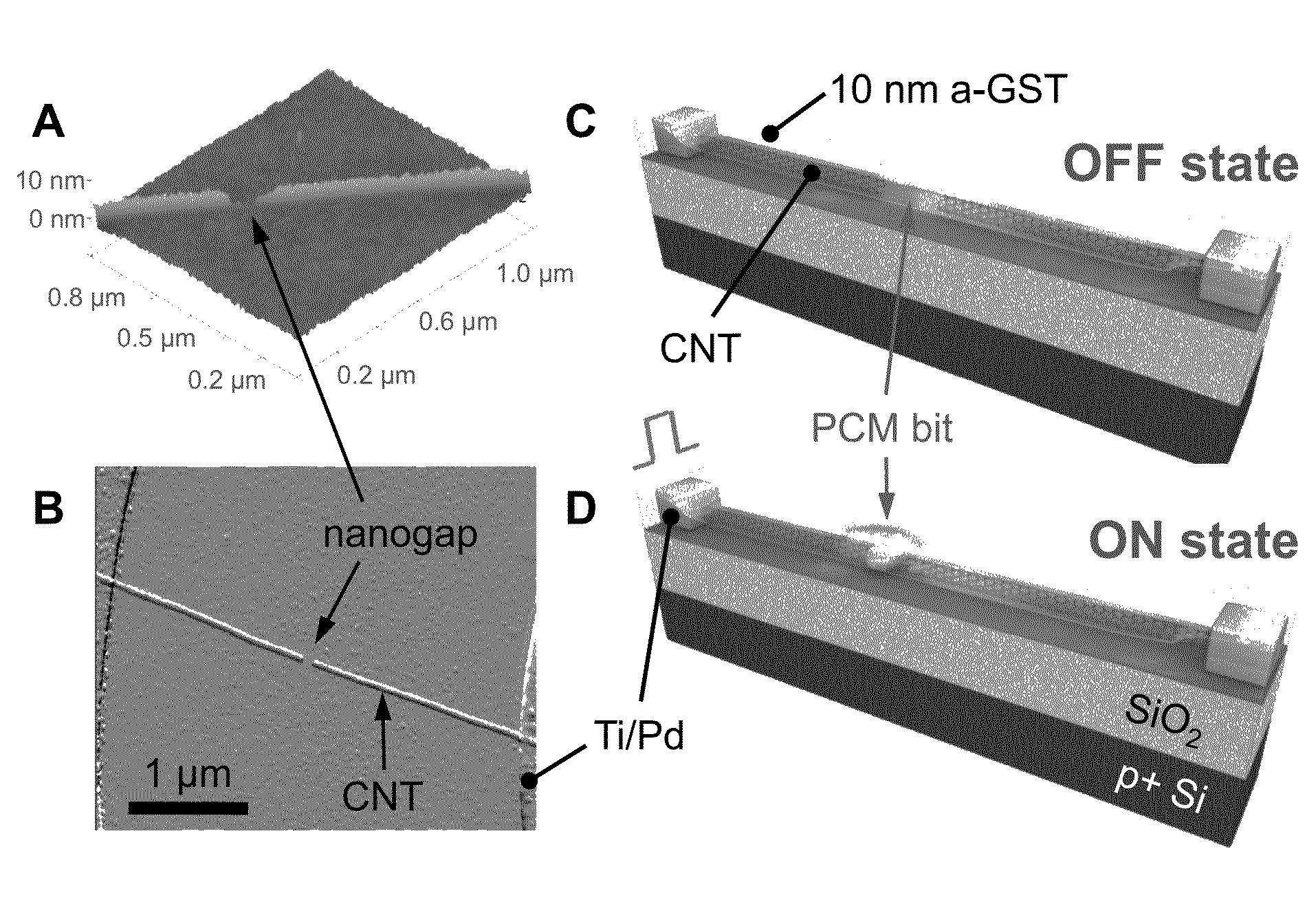
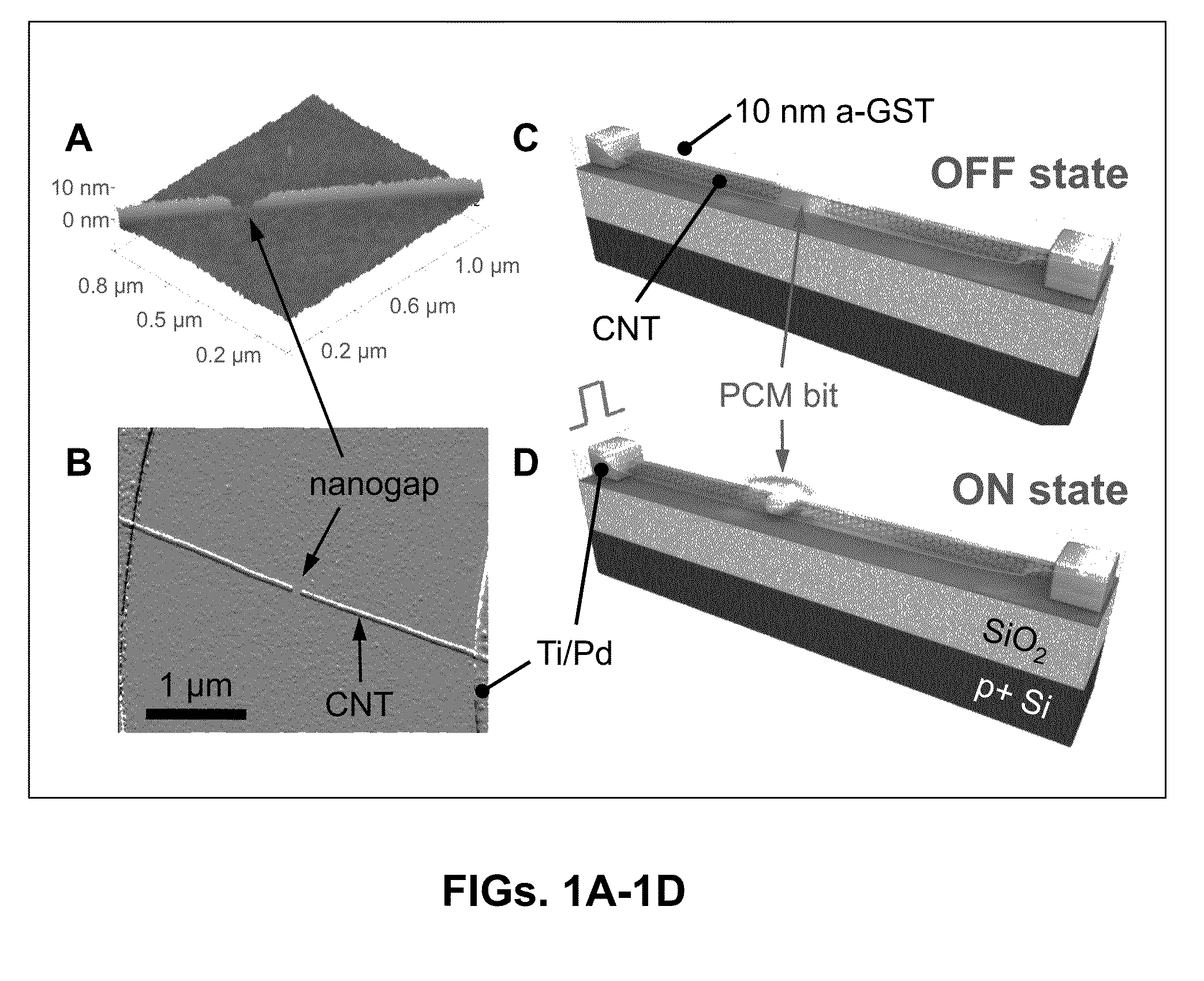
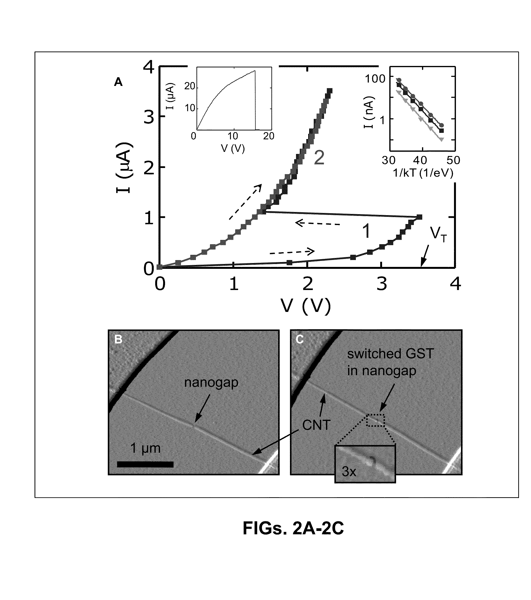
[0023]The subject disclosure can utilize or combine some or all embodiments described in U.S. patent application Ser. No. 12 / 463,953, filed on May 11, 2009, entitled, “Resistive Changing Device.” The aforementioned patent application is hereby incorporated by reference in its entirety.

[0024]One embodiment of the subject disclosure entails a device including a nanoelectrode having a gap, and a resistive change material located in the gap, wherein an application of a voltage potential across first and second terminals of the nanoelectrode causes the resistive change material to modify at least one non-volatile memory state of the resistive change material.

[0025]One embodiment of the subject disclosure entails a method for applying from a voltage source a first signal to a terminal of a nanoelectrode to program a non-volatile memory state of a resistive change material, where the resistive change material is located in a nanogap of the nanoelectrode. The method also includes receiving ...


PUM


Abstract

A system that incorporates teachings of the subject disclosure may include, for example, a device including a nanoelectrode having a gap, and a resistive change material located in the gap, wherein an application of a voltage potential across first and second terminals of the nanoelectrode causes the resistive change material to modify at least one non-volatile memory state of the resistive change material. Additional embodiments are disclosed.

Description

PRIOR APPLICATION[0001]The present application claims the benefit of priority to U.S. Provisional Application No. 60 / 476,578 filed on Apr. 18, 2011, entitled, “Phase-Change Memory Cell with Carbon Nanotube and Graphene Electrodes,” which is hereby incorporated by reference in its entirety.STATEMENT AS TO FEDERALLY SPONSORED RESEARCH[0002]This invention was made with government support under contract number N00014-09-0180 and N00014-10-1-0853 awarded by Office of Navy Research. The government has certain rights in the invention.FIELD OF THE DISCLOSURE[0003]The subject disclosure relates to an adaptive resistive device and methods thereof.BACKGROUND[0004]The mass-storage market is currently dominated by magnetic hard drives, which are typically used up to the terabyte range. In the gigabyte range, solid-state Flash memory is most commonly used. Hard drives contain movable parts and are slower, less robust, and more power-hungry than solid-state memory.[0005]Ideally, robust low-power t...

Claims


Application Information

Patent Timeline
IPC IPC(8): G11C11/00B82Y99/00
CPCG11C13/025G11C2213/35G11C2213/53B82Y10/00G11C13/0004H10N70/235H10N70/231H10N70/823H10N70/841H10N70/8828H10N70/026G11C13/0023G11C13/004
Inventor POP, ERICXIONG, FENGLIAO, ALBERT D.
Owner THE BOARD OF TRUSTEES OF THE UNIV OF ILLINOIS
Why Eureka
Eureka Blog
Learn More