Electron beam device

Inactive Publication Date: 2013-10-31
RIKEN
View PDF12 Cites 11 Cited by
  • Summary
  • Abstract
  • Description
  • Claims
  • Application Information

AI Technical Summary

Benefits of technology

[0018]The present invention is capable of controlling the in-plane distance between the electron beam transmitting through the specimen in the first region and the electron beam passing through the second region on the specimen plane, and each current density. The second electron biprism of the image forming system superposes the first electron beam and the second electron beam on

Problems solved by technology

Restriction of the coherence distance of the irradiation electron beam on the specimen plane may deteriorate contrast of the interference fringes as the width of the interference region is increased for observing inside of the thin film specimen.
Therefore, it is not possible to make the interference width wider than the coherence distance.
There has been a problem of difficulty in obtaining the image with reconstructed phase with high accuracy.
Besides, the specimen with large leakage magnetic fiel

Method used


Image

  • Electron beam device
  • Electron beam device
  • Electron beam device

Examples


first embodiment

[0060]A first Embodiment relates to the interference microscope using the transmission type electron microscope.

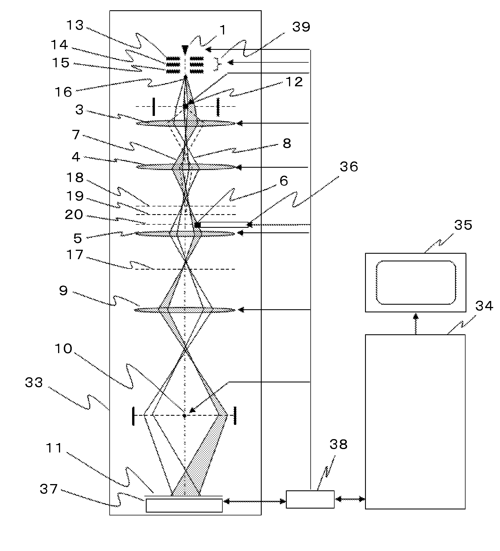
[0061]FIG. 3 schematically shows the optical system of the electron beam device according to the first embodiment. The electron beam device shown in FIG. 3 is intended to use the general purpose transmission type electron microscope for the interference microscope. However, the first embodiment is not limited to those described referring to the drawing. FIG. 4 shows the upper optical system of the electron beam device according to the first embodiment as shown in FIG. 3. FIG. 5 shows the relationship of the electron source on the electron optics, the first electrode filament plane on the electron optics, and the specimen plane. They have been already described, and explanations thereof will be omitted.

[0062]As for the electron beam device according to the first embodiment shown in FIG. 3, the electron source 1 is located at the most upstream part in the electron beam flow ...

second embodiment

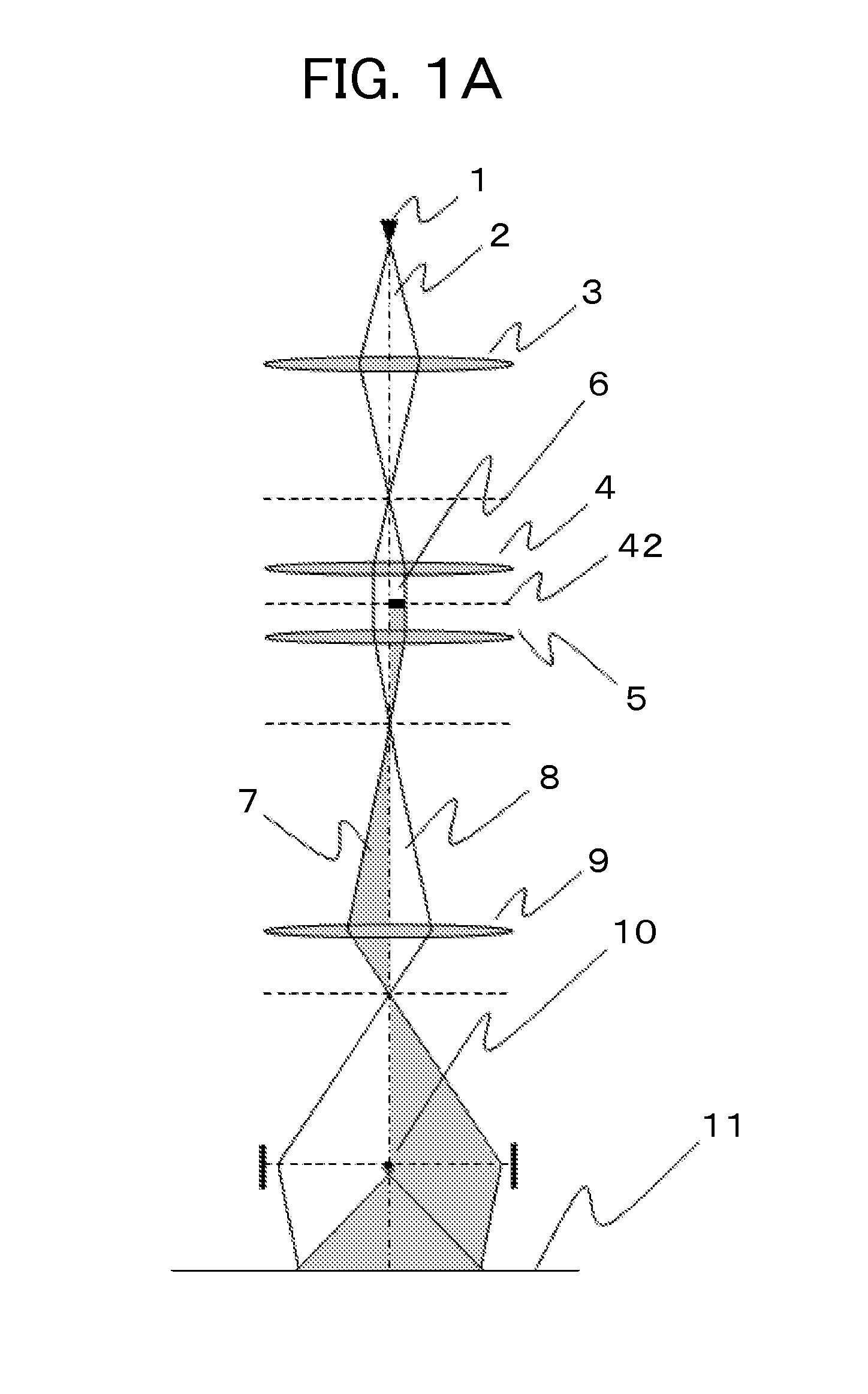
[0072]FIG. 6 is a schematic view showing an electron beam device according to a second embodiment. FIG. 7 is a schematic view showing an upper optical system of the electron beam device shown in FIG. 6. The overall structure of the device is similar to that of the first embodiment. Therefore, explanation of the same parts as those of the first embodiment will be omitted, and the upper optical system with different structure will be described.

[0073]Referring to the electron beam device according to the embodiment, that is, the interference microscope using the transmission type electron microscope, the first electron biprism is provided downstream of the first electron source and upstream of the electron lens of the irradiation system. However, as for the electron beam device as FIG. 7 clearly shows, the electron lens of the irradiation system is formed only of the first irradiation electron lens 3, while omitting the second irradiation electron lens 4. It is therefore possible to co...

third embodiment

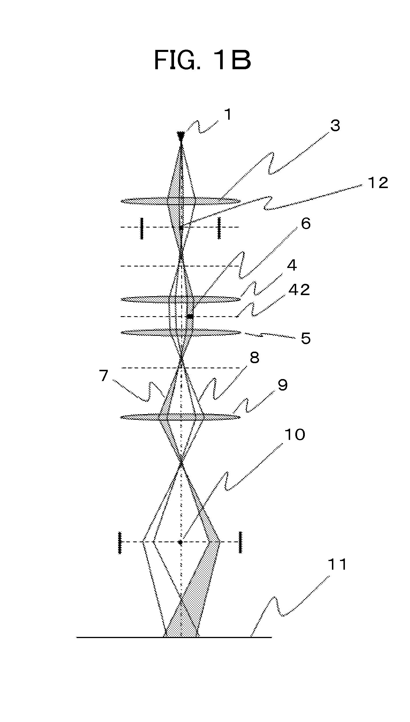
[0076]FIG. 8 is a schematic view showing an electron beam device according to a third embodiment. FIG. 9 shows an upper optical system of the electron beam device. As the overall structure of the electron beam device is similar to that of the first embodiment, explanation of the same parts as those of the first embodiment will be omitted. The upper optical system with different device structure will only be described. The upper optical system of the electron beam device according to this embodiment has the feature that the first electron biprism is provided inside the electron lens of the irradiation system, that is, between the first and the second irradiation electron lenses which constitute the electron lens of the irradiation system. Action of the second irradiation electron lens then serves to irradiate the specimen with parallel electron beams.

[0077]Referring to the electron beam device according to the third embodiment as FIG. 9 clearly shows, the first irradiation electron l...


PUM


Abstract

An electron beam device includes a first electron biprism between an acceleration tube and irradiation lens systems, and an electron biprism in the image forming lens system. The first electron biprism splits the electron beam into first and second electron beams, radiated to differently positioned first and second regions on objective plane of an objective lens system having a specimen perpendicular to an optical axis. The first and second electron beams are superposed on the observation plane by the electron biprism of the image forming lens system. The superposed region of those electron beams is observed or recorded. Optical action of the irradiation lens system controls each current density of the first and second electron beams on the objective plane of the objective lens system having the specimen, and distance on electron optics between the first electron biprism and the objective plane of the objective lens system having the specimen.

Description

CLAIM OF PRIORITY[0001]The present application claims priority from Japanese patent application JP2012-100545 filed on Apr. 26, 2012, the content of which is hereby incorporated by reference into this application.BACKGROUND OF THE INVENTION[0002]The present invention relates to a device using an electron beam, and more particularly, the present invention relates to electron beam interferomatic technology using an electron microscope.[0003]An electron interferometer is used for measuring the phase change of the electron beam as an approach that quantitatively measures the magnetic field of a substance or in vacuum. FIG. 1A shows an optical setup for interferometry for a generally employed electron holography. The electron beam 2 emitted from the electron source 1 advances as shown in the drawing. Current density is adjusted by the first irradiation electron lens 3 and the second irradiation electron lens 4. The specimen 6 is placed at one side of the optical axis between the second i...

Claims


Application Information

Patent Timeline
IPC IPC(8): H01J37/22
CPCH01J37/22H01J37/295H01J2237/2614
Inventor TANIGAKI, TOSHIAKIAIZAWA, SHINJIMATSUDA, TSUYOSHIHARADA, KENTAKAHASHI, YOSHIO
Owner RIKEN
Why Eureka
Try Eureka