
Patterned substrate and light emitting diode structure

a light-emitting diode and substrate technology, applied in the direction of thin material processing, semiconductor devices, electrical devices, etc., can solve the problems of less power consumption of led, long life span and rapid response, and relatively short on/off time, so as to increase the overall luminance

Inactive Publication Date: 2013-10-31
CRYSTALWISE TECH
View PDF0 Cites 3 Cited by
  • Summary
  • Abstract
  • Description
  • Claims
  • Application Information

AI Technical Summary

Benefits of technology

The patent text discusses a patterned substrate and LED structures that use this substrate. The substrate has gaps between protrusions, which leads to better distribution and scattering of the light from the LED. This increases the overall luminance of the LED. The horizontal LED fabricated with this patterned substrate has higher luminance due to the gaps. On the other hand, the vertical LED fabricated with this substrate is more cost-effective. The gaps serve as channels to fill chemicals and separate the substrate from the LED structure, which can reduce cost compared to conventional laser peeling.

Problems solved by technology

More specifically, LED consumes less power, has longer life span and responses rapidly.
On / Off time is relatively short for LED lighting.
The high temperature within the LED may compromise the overall performance and stability.

Method used


Image

  • Patterned substrate and light emitting diode structure
  • Patterned substrate and light emitting diode structure
  • Patterned substrate and light emitting diode structure

Examples


Embodiment Construction

[0021]The aforementioned illustrations and following detailed descriptions are exemplary for the purpose of further explaining the scope of the instant disclosure. Other objectives and advantages related to the instant disclosure will be illustrated in the subsequent descriptions and appended drawings.

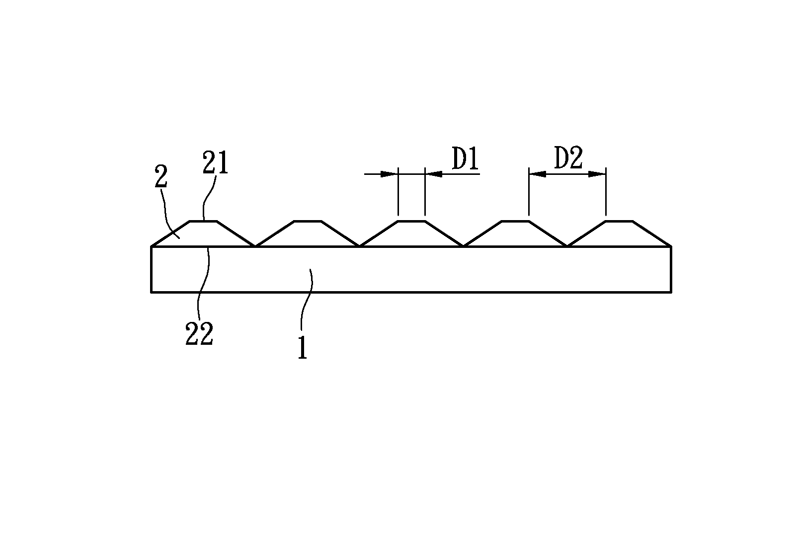
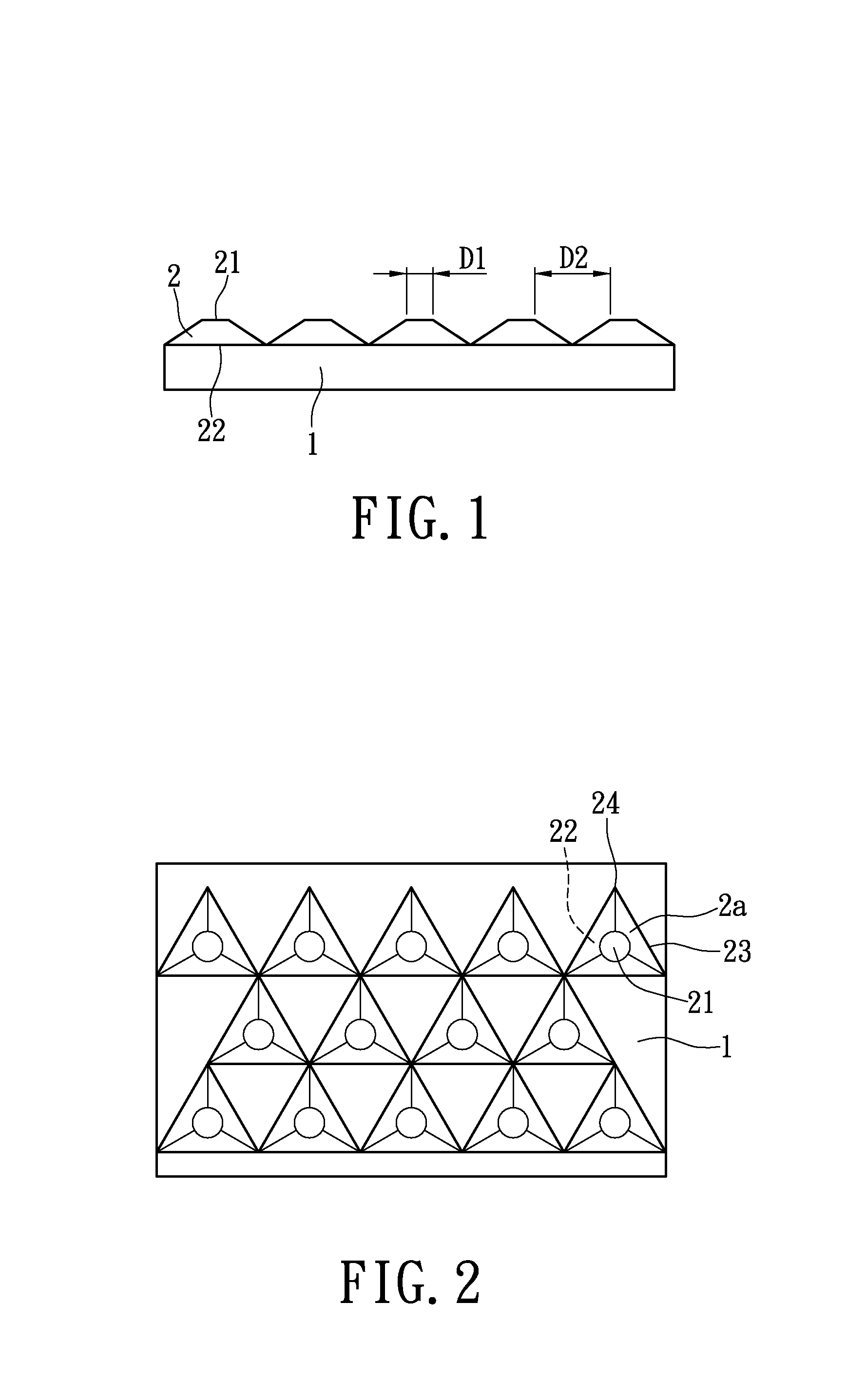
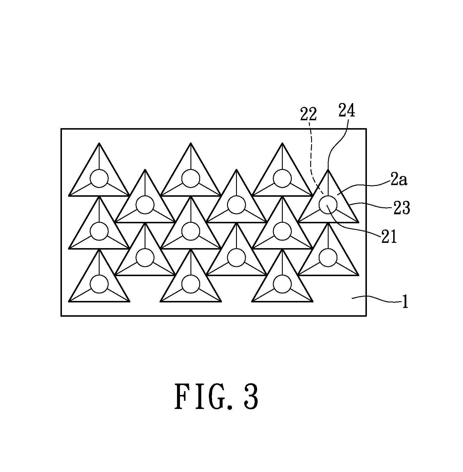
[0022]Please refer to FIG. 1. The instant disclosure provides a patterned substrate including a substrate 1 and a plurality of protrusions 2. The protrusions 2 extend from the substrate 1. Each protrusion 2 has a top face 21 and a base 22. The top face 21 of the protrusion 2 may be configured to a circle, triangle, diamond, polygonal configuration or any other geometric configurations and the instant disclosure is not limited thereto. The protrusions 2 are attached to the substrate via the base 22. The minimum distance between each pair of the immediately adjacent protrusions 2 is between 0 to 0.2 μm. However, when the pair of immediately adjacent protrusions 2 is parted by 0 μm, the t...


PUM


Abstract

A patterned substrate includes a substrate and a plurality of protrusions. The protrusions are formed on the substrate. Each protrusion has a top face and a base. Each pair of immediately adjacent protrusions is minimally parted by 0 to 0.2 μm. When the distance between the adjacent protrusions falls as 0 μm, the bases thereof contact each other. A horizontal and a vertical light emitting diode structures using the patterned substrate are also discussed.

Description

BACKGROUND[0001]1. Field of the Invention[0002]The instant disclosure relates to a substrate and a light emitting diode; in particular, to a patterned substrate and a light emitting diode using the same.[0003]2. Description of Related Art[0004]Light Emitting Diode (LED) is a lighting unit made of semiconductors. LED has two electrode terminals. When a voltage is applied to the terminals, small amount of current goes through LED and the combination of electrons and holes excites the rest energy as a form of light. This is the mechanism of LED light emitting. LED is different from the conventional incandescent light because LED is luminescence. More specifically, LED consumes less power, has longer life span and responses rapidly. On / Off time is relatively short for LED lighting. In addition, the size of LED is small and therefore suitable for mass production. It is easier to meet the practical demand such as smaller volume or matrix arrangement. The luminance of LED has been improved...

Claims


Application Information

Patent Timeline
Patent Type & Authority Applications(United States)
IPC IPC(8): H01L33/22
CPCH01L33/22H01L33/10Y10T428/24678
Inventor LIN, BO-WENHSU, SHIH-CHIEHPENG, CHUN-YENHSU, WEN-CHING
Owner CRYSTALWISE TECH
Learn More