

Multilayer ceramic electronic component and method of manufacturing the same
a technology of ceramic electronic components and multi-layer ceramics, applied in the manufacture of fixed capacitors, fixed capacitor details, fixed capacitors, etc., can solve the problems of deterioration of product reliability, affecting the reliability of products, so as to prevent insulation breakdown and cracks
- Summary
- Abstract
- Description
- Claims
- Application Information
AI Technical Summary
Benefits of technology
Problems solved by technology
Method used
Image

Examples
Embodiment Construction
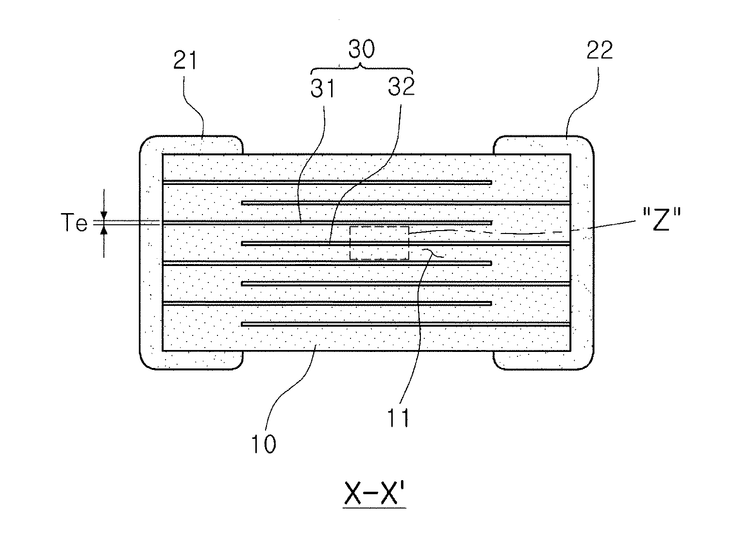
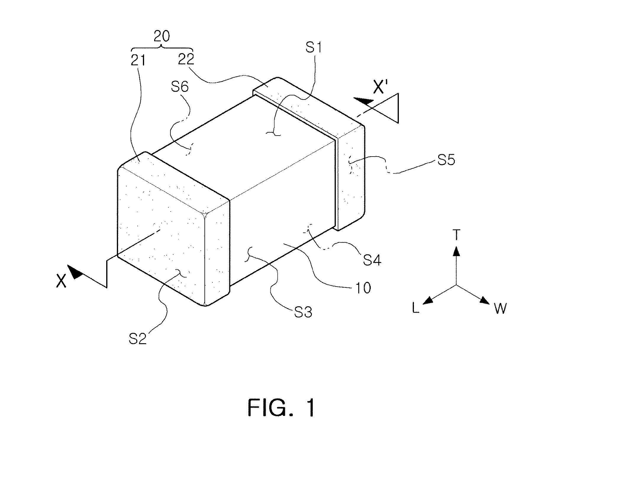
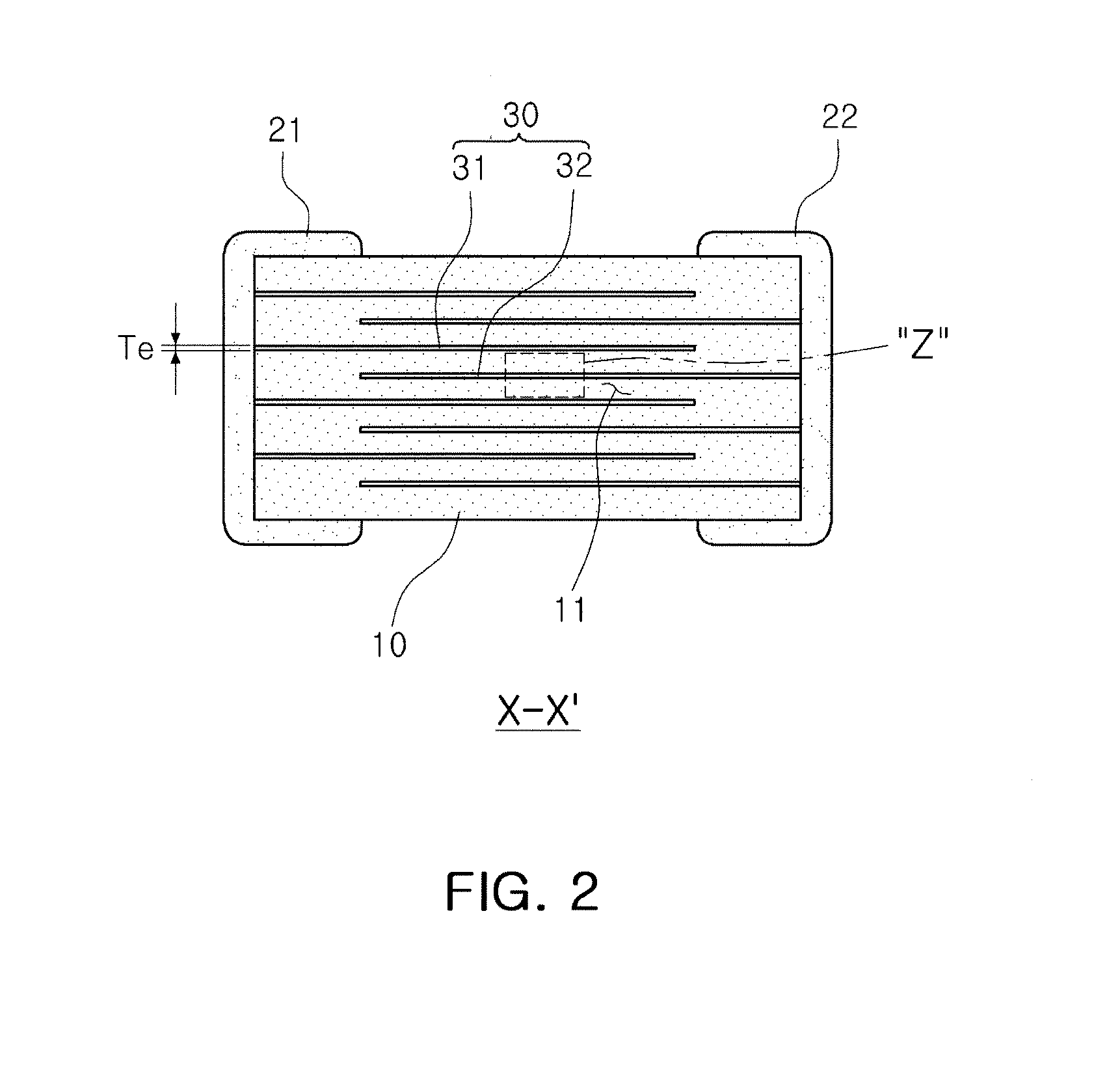
[0034]Embodiments of the present invention will now be described in detail with reference to the accompanying drawings.
[0035]The invention may, however, be embodied in many different forms and should not be construed as being limited to the embodiments set forth herein.
[0036]The embodiments of the present invention are provided so that those skilled in the art may more easily understand the present invention.
[0037]The terminology used herein is for the purpose of describing particular embodiments only and is not intended to limit the inventive concept. As used herein, the singular forms “a”“an” and “the” are intended to include the plural forms as well, unless the context clearly indicates otherwise.
[0038]In addition, unless explicitly described otherwise, “comprising” any components will be understood to imply the inclusion of other components but not the exclusion of any other components.
[0039]In the drawings, the shapes and dimensions may be exaggerated for clarity, and the same ...
PUM
| Property | Measurement | Unit |
|---|---|---|
| Length | aaaaa | aaaaa |
| Fraction | aaaaa | aaaaa |
| Fraction | aaaaa | aaaaa |
Abstract
Description
Claims
Application Information