Phase-stabilized thin films, structures and devices including the thin films, and methods of forming same

a technology of phase stabilization and thin films, applied in semiconductor devices, inorganic chemistry, chemistry apparatuses and processes, etc., can solve problems such as domain-specific work function differences, process problems, and inability to meet the requirements of feature-size-dependent performance variations, and achieve the effect of facilitating the formation of nitrogen-containing films

Active Publication Date: 2013-11-07
ASM IP HLDG BV
View PDF5 Cites 385 Cited by
  • Summary
  • Abstract
  • Description
  • Claims
  • Application Information

AI Technical Summary

Benefits of technology

[0008]Various embodiments of the present disclosure relate to phase-stabilized films, methods of forming phase-stabilized films, and structures and devices including the phase-stabilized films. The phase-stabilized films described herein may be used, for example, for gate electrodes and similar films in microelectronic devices. While the ways in which various embodiments of the disclosure address the drawbacks of the prior art methods and films is discussed in more detail below, in general, the disclosure provides phase-stabilized films that may have more desirable properties when used as a gate electrode in, for example, metal oxide semiconductor devices, compared to films that might otherwise form without a phase stabilizer. However, the invention is not necessarily limited to such applications.
[0009]In accordance with various embodiments of the disclosure, methods of forming phase-stabilized nitrogen-containing films include supporting a substrate in a reactor and forming a phase-stabilized nitrogen-containing film on an exposed surface of the substrate. In accordance with various aspects of these embodiments, a method includes the steps of supplying a phase stabilizer precursor and a matrix material precursor to an exposed surface of the substrate and supplying a nitrogen-containing reactant to the reactor so that the nitrogen-containing reactant reacts with active species on the exposed surface of the substrate to form the phase-stabilized film. The steps of supplying a phase stabilizer precursor and a matrix material precursor may be performed concurrently or may be performed as sequential pulses. In accordance with further aspects of these embodiments, the phase-stabilized nitrogen-containing film comprises a phase-stabilized metal nitride film. The phase-stabilized metal nitride film may be formed on a substrate supported in a reactor, where the phase-stabilized metal nitride film comprises a phase stabilizer that stabilizes a matrix material comprising a metal nitride into a selected solid phase. In this example, the phase-stabilized metal nitride film may be formed on the exposed surface of the substrate by concurrently or sequentially (e.g., pulsing) supplying a phase stabilizer precursor and a metal nitride precursor to an exposed surface of the substrate and then supplying a nitrogen-containing reactant to the reactor so that the nitrogen-containing reactant reacts with active species on the exposed surface of the substrate to from the phase-stabilized metal nitride film. In accordance with yet further aspects of these embodiments, the metal nitride film includes a group V transition metal, such as vanadium, niobium, or tantalum. And, in accordance with further aspects, the phase stabilizer comprises a group IV transition metal, such as titanium, zirconium, or hafnium and / or a group VI transition metal, such as chromium, molybdenum, or tungsten. And, in accordance with yet additional exemplary embodiments, the nitrogen-containing film comprises TaxTi(1−x)N. A treatment gas, such as hydrogen may be used during the formation of the film to facilitate formation of nitrogen-containing films having desired morphology and / or properties. The films formed in accordance with these methods may be used as gate electrodes or other layers within electronic devices.
[0010]In accordance with additional embodiments of the disclosure, a phase-stabilized nitrogen-containing film includes a solid solution having a stoichiometric ratio of MmzxMs(z−x)X, where MmX represents the matrix material and where Ms represents the phase stabilizer. MmX may be a first metal nitride (e.g., MmxNy) and Ms may be a second metal that stabilizes the matrix material into a selected phase. The matrix material MmxNy, may determine one or more electrical properties of the phase-stabilized film (e.g., a work function) while a second metal nitride MsxNy, may determine or affect morphological characteristics for the phase-stabilized film (e.g., a cubic phase), even if a native metal nitride metal nitride MmaNb would exhibit a different morphology under identical film formation conditions. In accordance with various aspects of these embodiments, X is nitrogen. In accordance with further aspects, Mm is one or more group V transition metals, such as vanadium, niobium, or tantalum. In accordance with further aspects, Ms includes one or more group IV transition metals, such as titanium, zirconium, or hafnium and / or group VI transition metal, such as chromium, molybdenum, and tungsten.
[0011]In accordance with yet additional embodiments of the disclosure, a structure, e.g., a semiconductor structure, includes a gate dielectric material and a metal gate electrode material comprising a solid solution formed overlying the gate dielectric material, the solid solution comprising a phase stabilizer that stabilizes a metal nitride in a solution phase that is different from a native phase of the metal nitride that would be formed under identical film formation conditions. The structure may additionally include a substrate, such as a semiconductor substrate, and additional layers typically used in the manufacture of electronic devices. In accordance with various aspects of these embodiments, the metal nitride material includes one or more group V transition metals. In accordance with further aspects, the phase stabilizer includes one or more group IV transition metals, such as titanium, zirconium, or hafnium and / or group VI transition metal, such as chromium, molybdenum, and tungsten. The metal nitride may determine one or more electrical properties of the phase-stabilized film (e.g., a work function) while the phase stabilizer may determine or affect morphological characteristics for the phase-stabilized film (e.g., a cubic phase). Structures in accordance with various aspects of these embodiments may be used to form electronic devices, such as metal oxide semiconductor devices.

Problems solved by technology

Although various processes for forming metal gate electrodes have been developed, many of these processes exhibit unacceptable feature-size dependent performance variations.
As a result, as the feature sizes of semiconductor devices decrease, these processes become increasingly problematic.
As a gate length becomes smaller in MOS devices, the domain size may occupy a relatively larger portion of gate electrode, potentially leading to domain-specific work function differences that may have a greater effect on the overall work function of the device.
In turn, there may be gate-to-gate work function variation that depends on the gate feature size, which may result in poor device performance.
Metal gate electrodes may also be difficult to integrate into device manufacturing processes because it can be difficult to deposit metal gate electrode films having desired film uniformity or other properties.
Depositing thin films of metal gate electrode material on the sidewalls of such structures may be challenging when using some existing deposition processes approaches.
For example, mass transport phenomena inherent in physical vapor deposition (PVD) and chemical vapor deposition (CVD) techniques may provide poor step coverage in such structures and may lead to inconsistent film thickness as a function of the gate dielectric supporting structure height.
Further, because some properties of a material that may make it attractive as a potential metal gate electrode material may not be present in a thermodynamically stable phase of the material, it may be difficult to form a desirable but less stable phase of the material using traditional PVD and CVD techniques.
For example, a PVD deposition may lead to a film initially having identical composition as the target or targets, and the high energies involved in the PVD process may lead to equilibration into a more thermodynamically stable form of the material, which has less desirable work function properties.
As another example, attempts to form desirable metastable phases of material with CVD processes may lead to incomplete conversion and within substrate compositional non-uniformities, potentially leading to downstream processing difficulties and / or device performance problems.

Method used


Image

  • Phase-stabilized thin films, structures and devices including the thin films, and methods of forming same
  • Phase-stabilized thin films, structures and devices including the thin films, and methods of forming same
  • Phase-stabilized thin films, structures and devices including the thin films, and methods of forming same

Examples


Embodiment Construction

[0020]The description of exemplary embodiments of methods, structures, and devices provided below is merely exemplary and is intended for purposes of illustration only; the following description is not intended to limit the scope of the disclosure or the claims. Moreover, recitation of multiple embodiments having stated features is not intended to exclude other embodiments having additional features or other embodiments incorporating different combinations of the stated features.

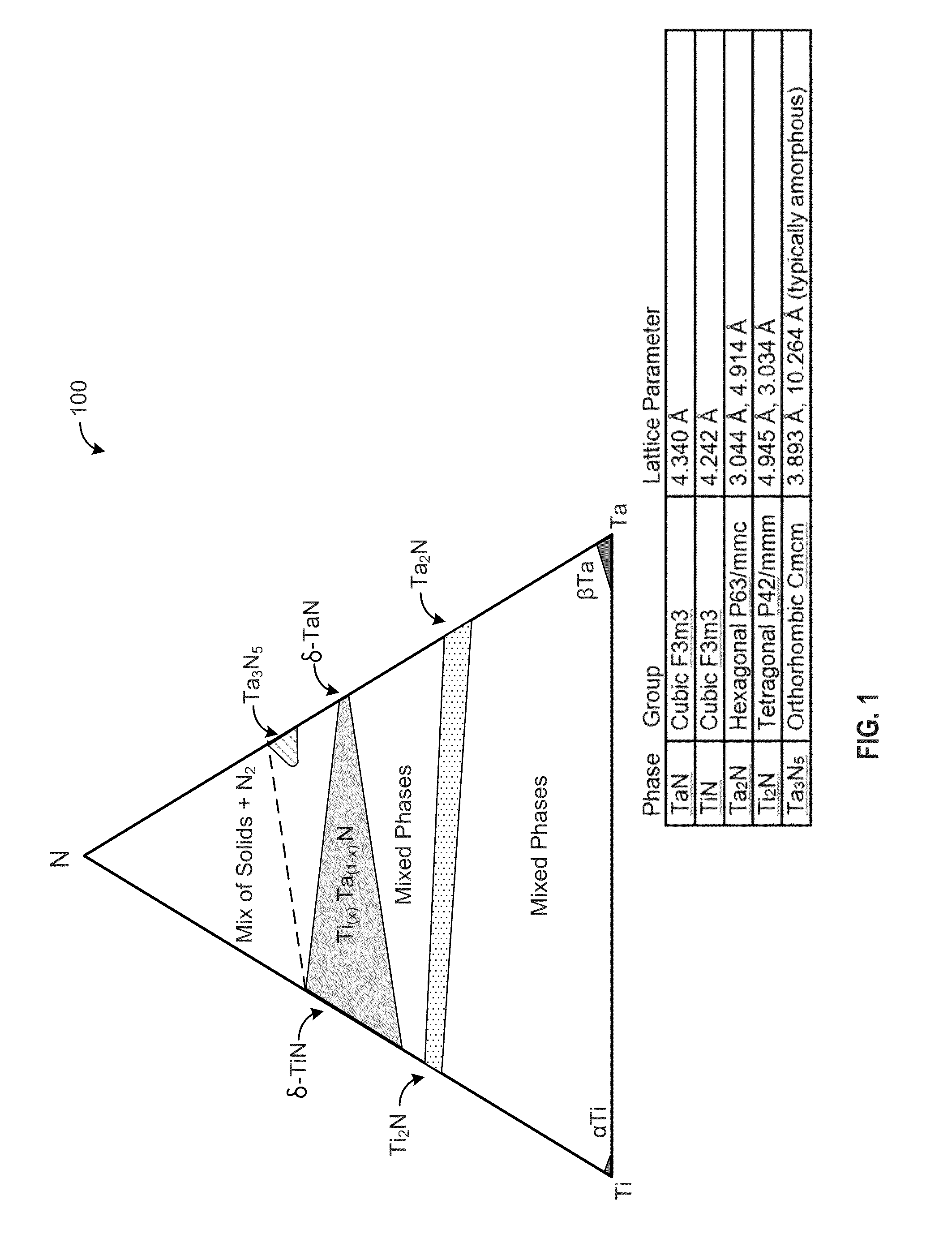
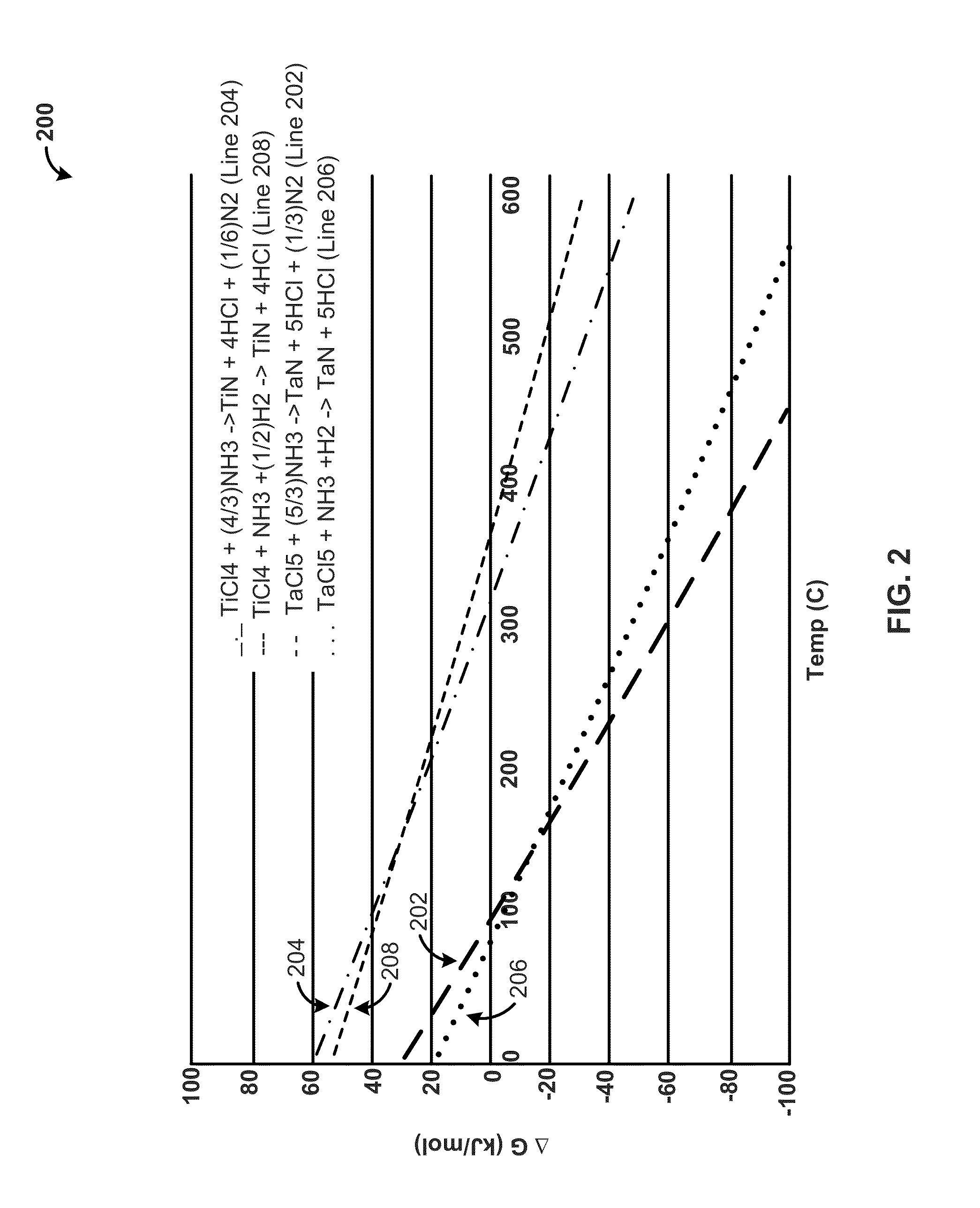
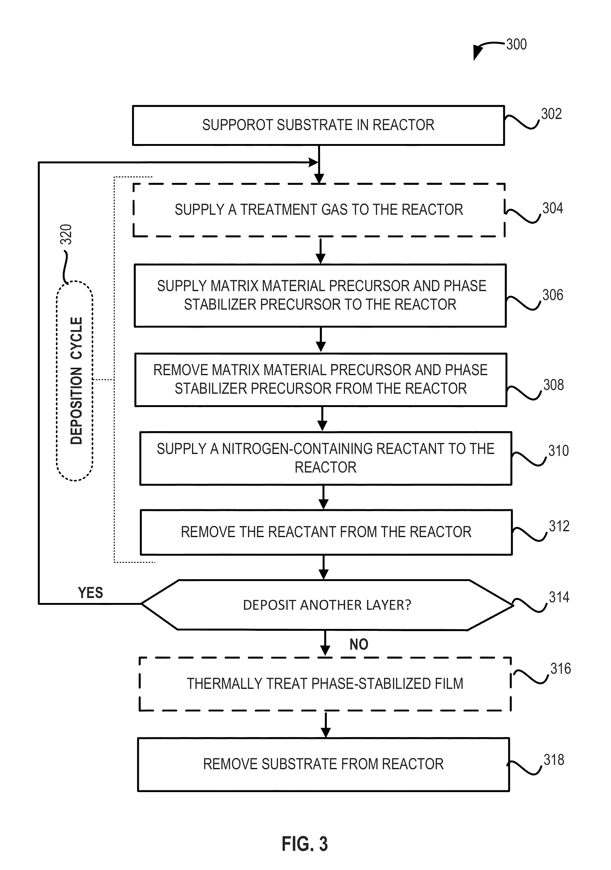
[0021]The present disclosure relates, generally, to nitrogen-containing phase-stabilized films, to methods of forming the films, and to structures and devices including the films. As set forth in more detail below, nitrogen-containing phase-stabilized films in accordance with various embodiments of the disclosure include a phase stabilizer to stabilize a solid phase of the nitrogen-containing films. It will be appreciated that the embodiments disclosed herein may be used to form any suitable phase-stabilized...


PUM

PropertyMeasurementUnit
temperaturesaaaaaaaaaa
temperatureaaaaaaaaaa

Abstract

Nitrogen-containing phase-stabilized films, methods of forming phase-stabilized films, and structures and devices including the phase-stabilized films are disclosed. The phase-stabilized films include a matrix material and a phase stabilizer, which provides a morphologically stabilizing effect to a matrix material within the films. The phase-stabilized films may be used as, for example, gate electrodes and similar films in microelectronic devices.

Description

CROSS REFERENCE TO RELATED APPLICATION[0001]This application claims the right of priority based on U.S. Provisional Patent Application No. 61 / 641,602 entitled “FORMATION OF PHASE-STABILIZED THIN FILMS,” filed on May 2, 2012, which is incorporated herein by reference, to the extent it does not conflict with the present disclosure.FIELD OF INVENTION[0002]The present disclosure generally relates to thin-film deposition techniques. More particularly, the disclosure relates to thin films including a phase stabilizer, to structures and devices including the films, and to methods of forming the films, structures, and devices.[0003]BACKGROUND OF THE DISCLOSURE[0004]Many semiconductor devices include non-silicon work function materials. For example, metal-oxide semiconductor (MOS) devices may include a gate electrode that includes a metal to assist in setting the effective work function for the gate electrode. Use of metal-containing electrodes in such devices has become increasingly importa...

Claims


Application Information

Patent Timeline
Patent Type & Authority Applications(United States)
IPC IPC(8): H01L29/49H01L29/40
CPCH01L29/4908H01L29/401H01L21/28088H01L21/67167H01L21/67253H01L29/4966H01L29/517
Inventor MILLIGAN, ROBERT BRENNANALOKOZAI, FRED
Owner ASM IP HLDG BV
Why Eureka
Try Eureka