Light-Emitting Device and Electronic Device

a technology of light-emitting devices and electronic devices, which is applied in the direction of electroluminescent light sources, thermoelectric devices, electric lighting sources, etc., can solve the problems of damage to the transistor or the organic el element due to bending or curving, damage to the display defect of a light-emitting device, etc., and achieves high flexibility, high reliability of light-emitting devices, and suppression of damage to transistors or organic el elements due to bending or

Active Publication Date: 2013-11-14
SEMICON ENERGY LAB CO LTD
View PDF3 Cites 131 Cited by
  • Summary
  • Abstract
  • Description
  • Claims
  • Application Information

AI Technical Summary

Benefits of technology

[0055]In a light-emitting device of one embodiment of the present invention, a difference between stress applied to a transistor and stress applied to an organic EL element when physical power is externally applied is small, and the values of the stresses are also small. Therefore, damage to the transistor or the organic EL element due to bending or curving can be suppressed, thereby achieving a highly reliable light-emitt

Problems solved by technology

In a light-emitting device including a flexible substrate, however, stress is applied to a transistor and an organic EL element when physical force, such as bending or curving, is externally applied, and thus these elements are damaged in some cases.
Damage of any one of a transis

Method used


Image

  • Light-Emitting Device and Electronic Device
  • Light-Emitting Device and Electronic Device
  • Light-Emitting Device and Electronic Device

Examples


embodiment 1

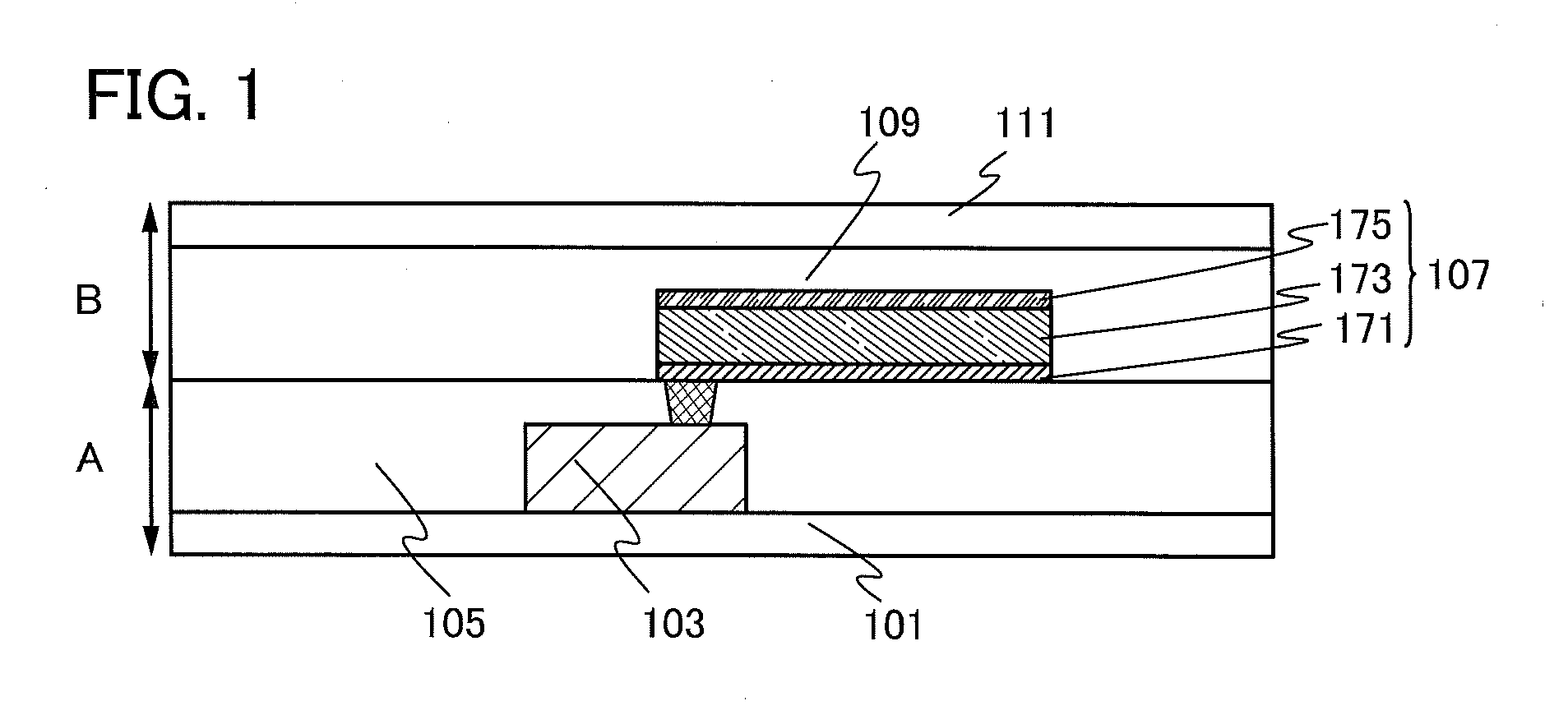
[0080]In this embodiment, light-emitting devices of embodiments of the present invention will be described with reference to FIG. 1 and FIGS. 2A and 2B.

[0081]FIG. 1 is a schematic view of a light-emitting device of one embodiment of the present invention. The light-emitting device illustrated in FIG. 1 includes, between one surface of a first flexible substrate 101 and one surface of a second flexible substrate 111, a planarization layer 105, a transistor 103 provided on the one surface side of the planarization layer 105, an organic EL element 107 provided on the other surface side of the planarization layer 105, and an adhesive layer 109 for bonding the first flexible substrate 101 and the second flexible substrate 111 with the transistor 103, the planarization layer 105, and the organic EL element 107 are provided therebetween. The organic EL element 107 is provided on and in contact with the other surface of the planarization layer 105, and includes a first electrode 171 electri...

embodiment 2

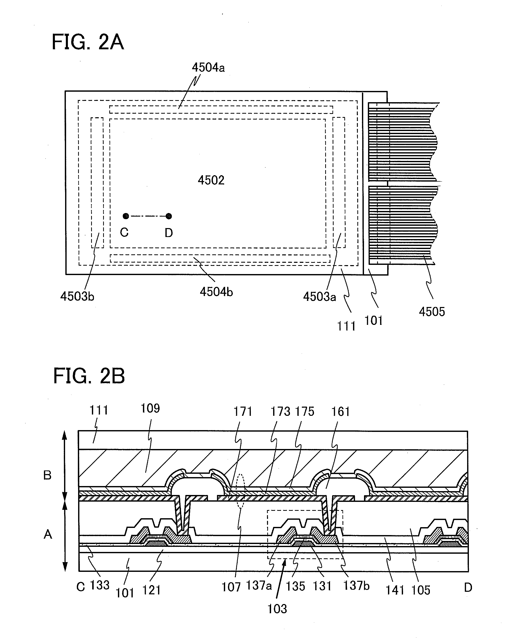
[0120]In this embodiment, a light-emitting device of one embodiment of the present invention will be described with reference to FIGS. 3A and 3B, FIGS. 4A and 4B, FIGS. 5A to 5E, and FIGS. 6A to 6E.

[0121]The light-emitting device of this embodiment is manufactured by a technique in which an element such as a transistor is manufactured over a formation substrate, and then the element is transferred from the formation substrate to a flexible substrate.

[0122]FIGS. 3A and 3B illustrate an example of a specific structure of a light-emitting device to which one embodiment of the present invention is applied. FIG. 3A is a plan view of a light-emitting device of one embodiment of the present invention. The light-emitting device illustrated in FIG. 3A includes the pixel portion 4502, a signal line driver circuit 4503, a scan line driver circuit 4504, and the FPC 4505. FIG. 3B is a cross-sectional view taken along an alternate long and short dash line E-F in FIG. 3A.

[0123]The light-emitting d...

embodiment 3

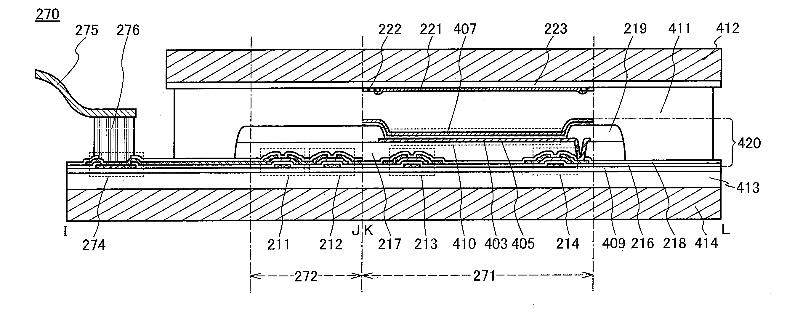
[0184]In this embodiment, a light-emitting device of one embodiment of the present invention will be described with reference to FIG. 7, FIG. 8, and FIG. 9.

[0185]FIG. 7 is a schematic cross-sectional view of a light-emitting device 400 described as an example in this embodiment.

[0186]The light-emitting device 400 includes an element layer 420 including a light-emitting element 410 provided over the substrate 401, a first protection layer 411 covering the element layer 420, and a second protection layer 412 provided over the first protection layer 411.

[0187]The substrate 401 has flexibility. The light-emitting element 410 is formed over an insulating surface of the substrate 401.

[0188]The light-emitting element 410 is a stack in which a first electrode 403, an EL layer 405, and a second electrode 407 are stacked in this order over the substrate 401. The EL layer 405 includes at least a light-emitting organic compound. At least one of the first electrode 403 and the second electrode 4...


PUM


Abstract

A highly reliable light-emitting device is provided. Damage to an element due to externally applied physical power is suppressed. Alternatively, in a process of pressure-bonding of an FPC, damage to a resin and a wiring which are in contact with a flexible substrate due to heat is suppressed. A neutral plane at which stress-strain is not generated when a flexible light-emitting device including an organic EL element is deformed, is positioned in the vicinity of a transistor and the organic EL element. Alternatively, the hardness of the outermost surface of a light-emitting device is high. Alternatively, a substrate having a coefficient of thermal expansion of 10 ppm/K or lower is used as a substrate that overlaps with a terminal portion connected to an FPC.

Description

BACKGROUND OF THE INVENTION[0001]1. Field of the Invention[0002]The present invention relates to a light-emitting device, an electronic device, and a lighting device each using organic electroluminescence (hereinafter also referred to as EL).[0003]2. Description of the Related Art[0004]In recent years, research and development have been actively conducted on light-emitting elements utilizing organic EL (organic EL elements). In the fundamental structure of the organic EL element, a layer containing a light-emitting organic compound (EL layer) is sandwiched between a pair of electrodes.[0005]Since the organic EL element is a self-luminous type, a light-emitting device including the organic EL element has advantages of high visibility, no necessity of a backlight, low power consumption, and the like. In addition, the light-emitting device including the organic EL element also has advantages that it can be thin and lightweight and it is highly responsive to input signals.[0006]Furtherm...

Claims


Application Information

Patent Timeline
IPC IPC(8): H01L51/52H05B44/00
CPCH01L51/5246H10K59/38H10K59/12H10K59/131H10K77/111H10K50/8426H10K50/865H10K50/844H10K2102/311H10K2102/351H10K50/30H10K71/00H10K50/8445H10K50/84H10K59/124
Inventor YAMAZAKI, SHUNPEIEGUCHI, SHINGO
Owner SEMICON ENERGY LAB CO LTD
Why Eureka
Try Eureka