Trench mosfet structures using three masks process

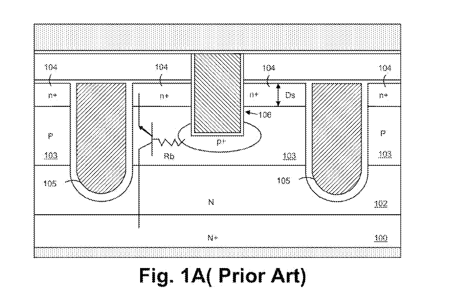
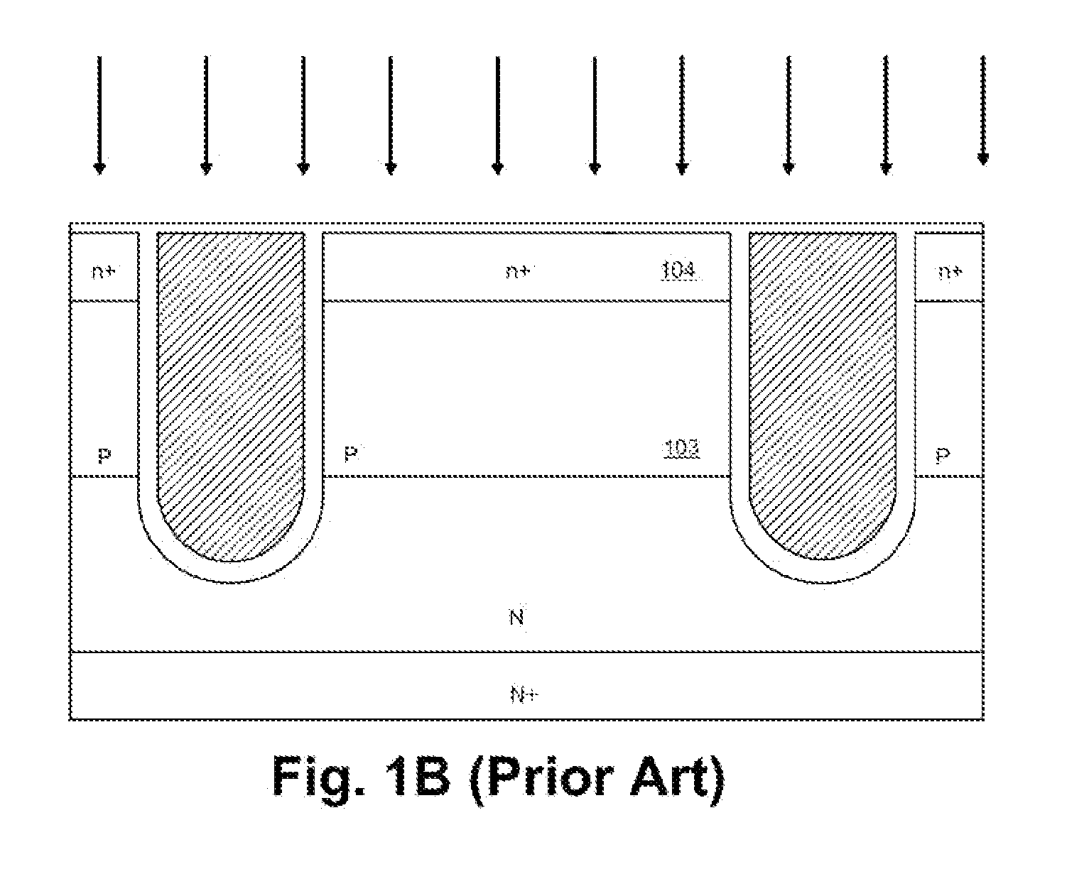
a mosfet and mask technology, applied in the field of mosfet structure, can solve the problems of reducing the emitter injection efficiency of parasitic npn and rendering it difficult to turn

Inactive Publication Date: 2013-11-14
HSIEH FU YUAN +1
View PDF6 Cites 3 Cited by
  • Summary
  • Abstract
  • Description
  • Claims
  • Application Information

AI Technical Summary

Benefits of technology

[0017]According to an added feature of the present invention, in some preferred embodiments, as shown in FIG. 17˜FIG. 19, a second TiN layer is added sandwiched between a barrier layer of Ti/TiN and a metal plug to avoid the possible TiN void occurring in corners of the trenched source-body contact structure.
[0018]The present invention further provides a method for manufacturing a trench MOSFET comprising a plurality of transistor cells with each comprising a plurality of trenched gates surrounded by source regions of a first conductivity type near a top surface of a silicon layer of the first conductivity type encompassed in body regions of a second conductivity type, the method comprising: depositing a contact interlayer on the

Problems solved by technology

Therefore, s Source Ballast Resistance (SBR) of the n region exists at cell corners, which reduces the Emitter injection efficiency of the parasitic NPN bip

Method used


Image

  • Trench mosfet structures using three masks process
  • Trench mosfet structures using three masks process
  • Trench mosfet structures using three masks process

Examples


Embodiment Construction

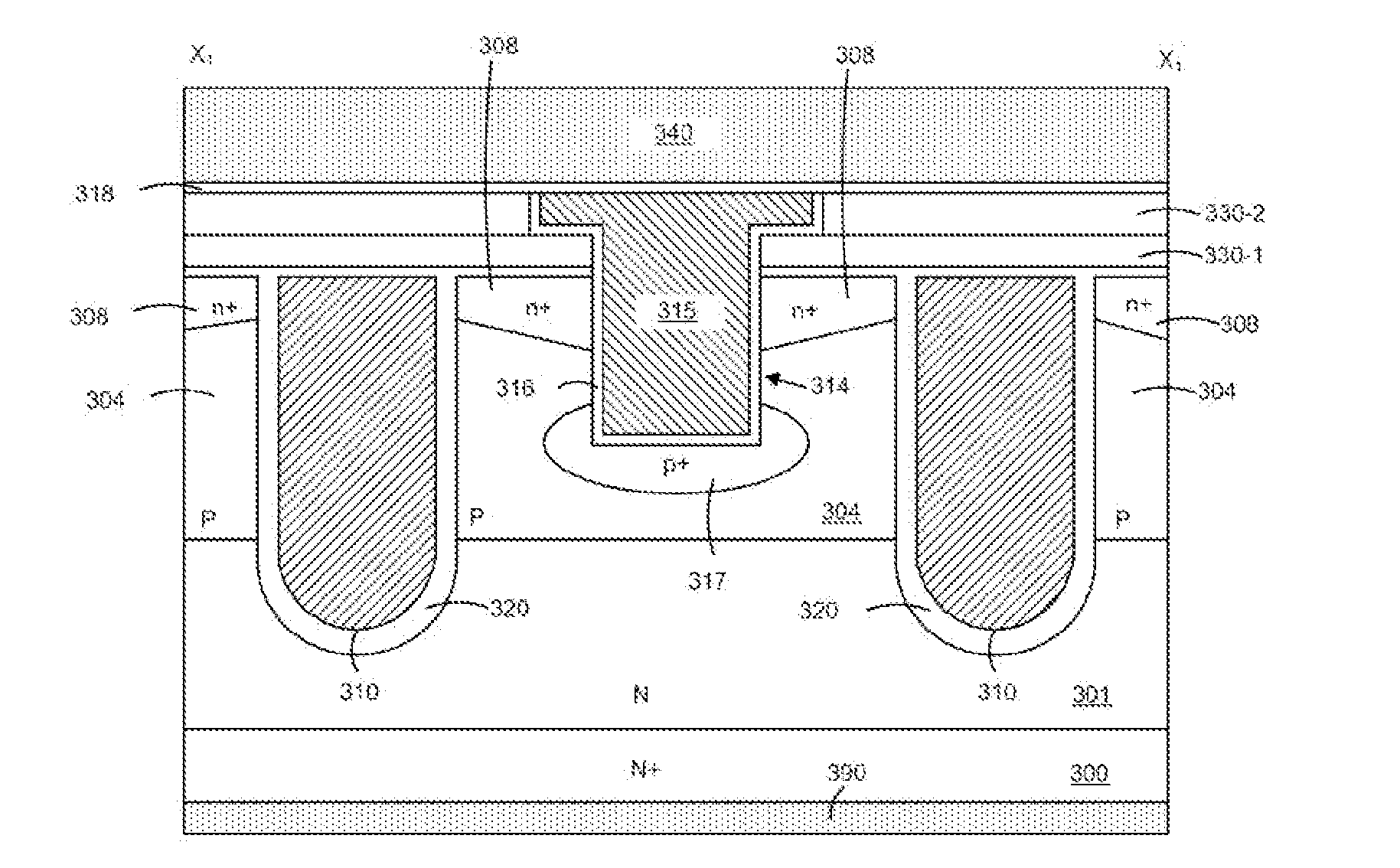
[0054]In the following Detailed Description, reference is made to the accompanying drawings, which forms a part thereof, and in which is shown by way of illustration specific embodiments in which the invention may be practiced. In this regard, directional terminology, such as “top”, “bottom”, “front”, “back”, etc., is used with reference to the orientation of the Figure(s) being described. Because components of embodiments can be positioned in a number of different orientations, the directional terminology is used for purpose of illustration and is in no way limiting. It is to be understood that other embodiments may be utilized and structural or logical changes may be make without departing from the scope of the present invention. The following detailed description, therefore, is not to be taken in a limiting sense, and the scope of the present invention is defined by the appended claims. It is to be understood that the features of the various exemplary embodiments described herein...


PUM


Abstract

A trench MOSFET comprising a plurality of trenched gates surrounded by source regions encompassed in body regions in active area. A plurality of trenched source-body contact structure penetrating through the source regions and extending into the body regions, are filled with tungsten plugs padded with a Ti layer, a first and a second TiN layer, wherein the second TiN layer is deposited after Ti silicide formation to avoid W spiking occurrence.

Description

CROSS REFERENCE TO RELATED APPLICATIONS[0001]This application is a Continuation-In-Part (CIP) of U.S. patent application Ser. No. 13 / 248,479 of the same inventor, filed on Sep. 29, 2011, entitled “METHOD OF MANUFACTURING TRENCH MOSFET STRUCTURES USING THREE MASKS PROCESS”, which is a divisional of U.S. patent application Ser. No. 12 / 654,327 filed on Dec. 17, 2009, now U.S. Pat. No. 8,058,685, which is a Continuation-In-Part of U.S. patent application Ser. No. 12 / 458,293 filed on Jul. 8, 2009, now U.S. Pat. No. 7,816,720.FIELD OF THE INVENTION[0002]This invention relates generally to the cell structures and device configuration of power semiconductor devices. More particularly, this invention relates to a novel and improved trench MOSFET (metal oxide semiconductor field effect transistor, the same hereinafter).BACKGROUND OF THE INVENTION[0003]Please refer to FIG. 1A for an active area of an N-channel trench MOSFET of a prior art (U.S. Pat. No. 6,888,196) with n+ source regions 104 ha...

Claims


Application Information

Patent Timeline
IPC IPC(8): H01L29/78H01L29/66
CPCH01L29/7813H01L29/66734H01L21/823437H01L21/823462H01L27/088H01L29/0696H01L29/086H01L29/0869H01L29/1095H01L29/407H01L29/41766H01L29/4236H01L29/4238H01L29/456H01L29/66727H01L29/7803H01L29/7811
Inventor HSIEH, FU-YUAN
Owner HSIEH FU YUAN
Why Eureka
Try Eureka