Pixel circuits including feedback capacitors and reset capacitors, and display systems therefore

a pixel circuit and feedback capacitor technology, applied in the direction of cathode-ray tube indicators, instruments, electric digital data processing, etc., can solve the problems of reducing the application voltage of the display panel, and reducing the uniformity of the display panel

Active Publication Date: 2013-11-14
IGNIS INNOVATION
View PDF31 Cites 44 Cited by
  • Summary
  • Abstract
  • Description
  • Claims
  • Application Information

AI Technical Summary

Problems solved by technology

TFTs fabricated on poly-silicon tend to demonstrate non-uniform behavior across display panels and over time.
Furthermore, emissive devices degrade over time and may require increasing applied voltage to maintain luminance levels, over time.
For example, additional lines and transistors associated with each pixel circuit may allow for additional compensation leading to greater uniformity, yet undesirably decrease pixel density.

Method used


Image

  • Pixel circuits including feedback capacitors and reset capacitors, and display systems therefore
  • Pixel circuits including feedback capacitors and reset capacitors, and display systems therefore
  • Pixel circuits including feedback capacitors and reset capacitors, and display systems therefore

Examples


Embodiment Construction

[0031]One or more currently preferred embodiments have been described by way of example. It will be apparent to persons skilled in the art that a number of variations and modifications can be made without departing from the scope of the invention as defined in the claims.

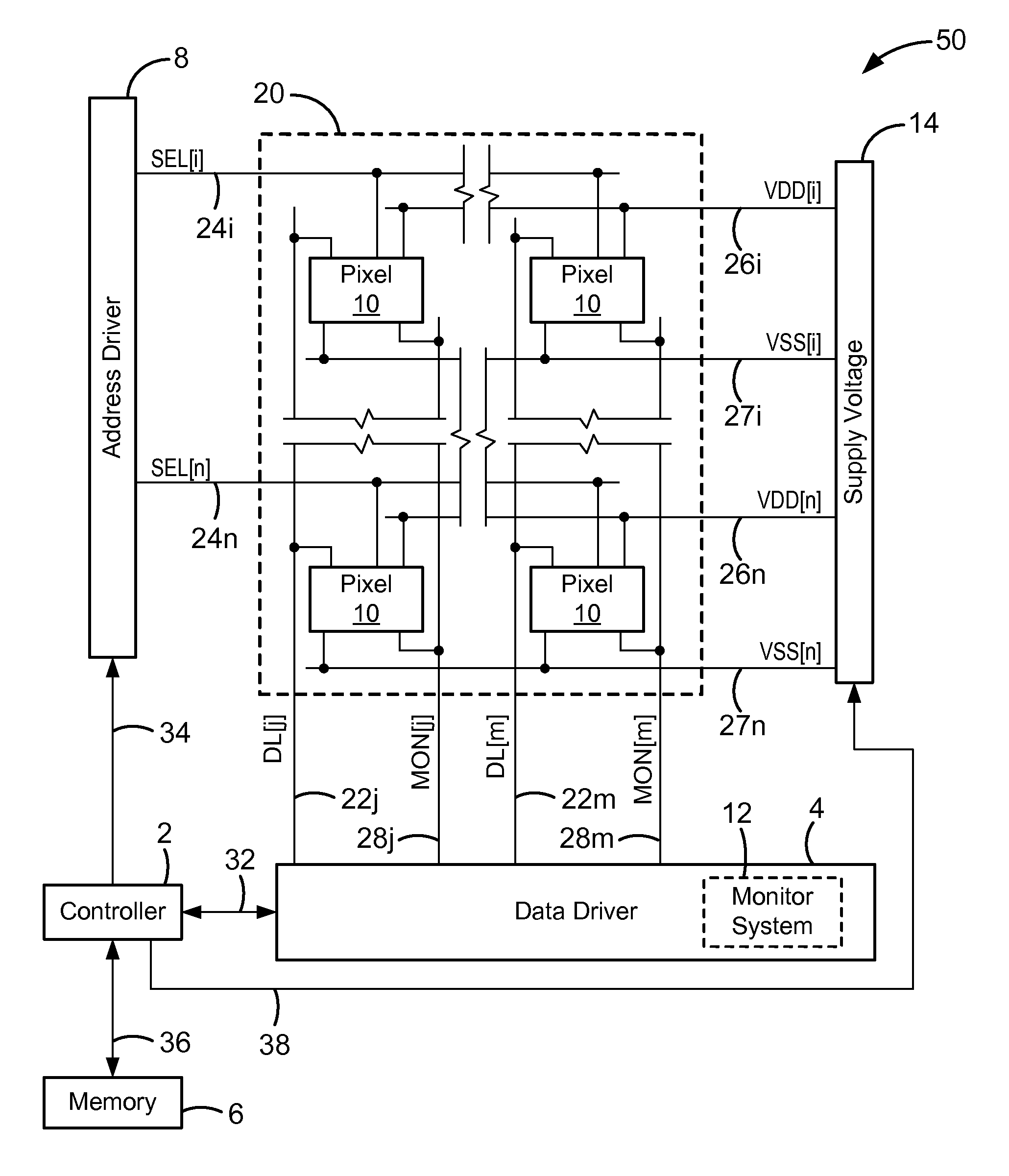
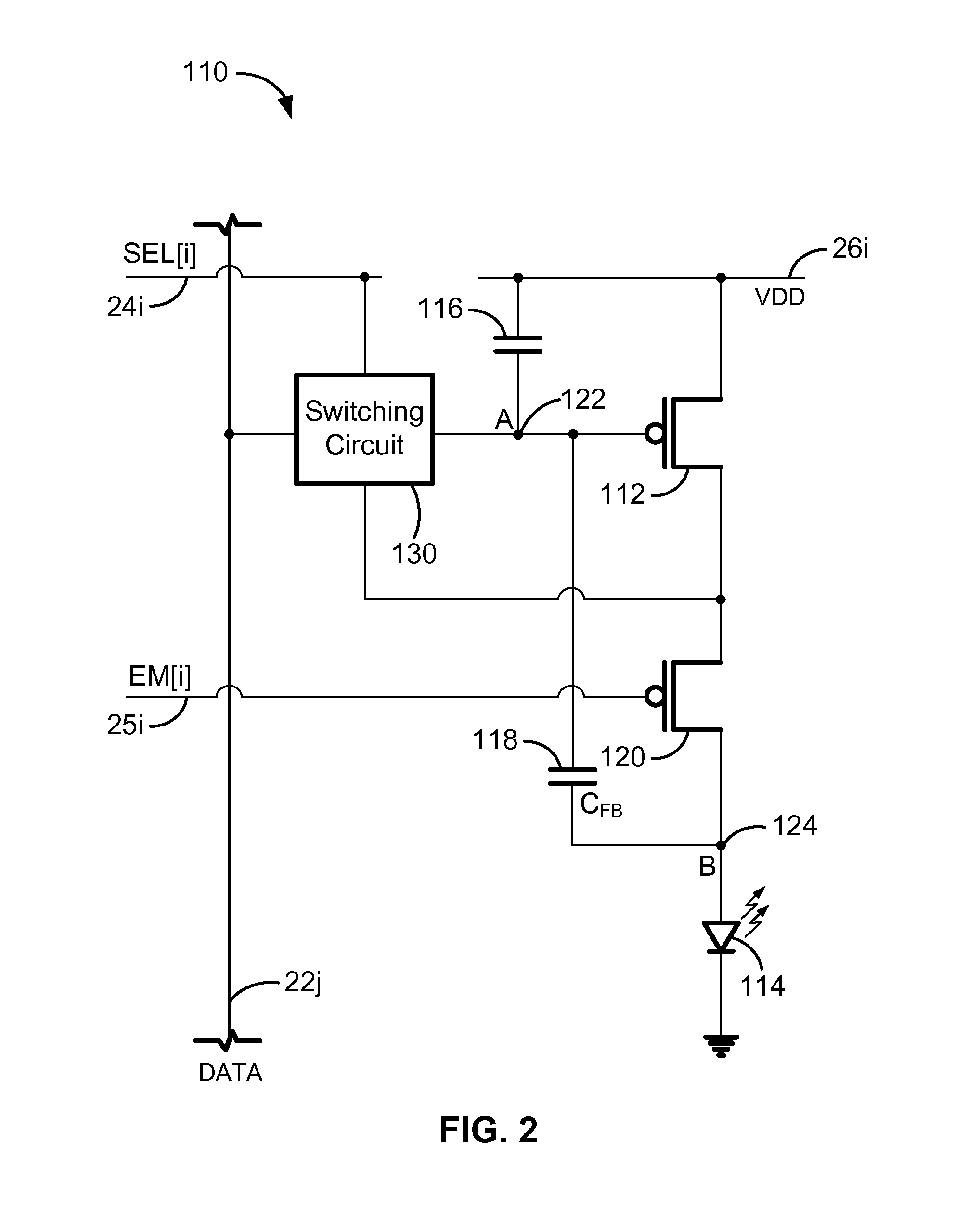
[0032]Embodiments of the present invention are described using a display system that may be fabricated using different fabrication technologies including, for example, but not limited to, amorphous silicon, poly silicon, metal oxide, conventional CMOS, organic, anon / micro crystalline semiconductors or combinations thereof. The display system includes a pixel that may have a transistor, a capacitor and a light emitting device. The transistor may be implemented in a variety of materials systems technologies including, amorphous Si, micro / nano-crystalline Si, poly-crystalline Si, organic / polymer materials and related nanocomposites, semiconducting oxides or combinations thereof. The capacitor can have different structu...


PUM


Abstract

A display with a pixel circuit for driving a current-driven emissive element includes a feedback capacitor in series between the emissive element and a programming node of the pixel circuit. During driving, variations in the operating voltage of the emissive element due to variations in the current conveyed through the emissive element by a driving transistor are accounted for. The feedback capacitor generates voltage adjustments at the programming node that correspond to the variations at the emissive element, and thus reduces variations in light emission. A reset capacitor connected to a select line is selectively connected to the gate terminal of the driving transistor and resets the driving transistor prior to programming. The select line adjusts the voltage on the gate terminal to reset the driving transistor by the capacitive coupling of the select line to the gate terminal created by the reset capacitor.

Description

FIELD OF THE INVENTION[0001]The present disclosure generally relates to circuits and methods of driving, calibrating, and programming displays, particularly displays including emissive elements and drive transistors therefore such as active matrix organic light emitting diode displays.BACKGROUND[0002]Displays can be created from an array of light emitting devices each controlled by individual circuits (i.e., pixel circuits) having transistors for selectively controlling the circuits to be programmed with display information and to emit light according to the display information. Thin film transistors (“TFTs”) fabricated on a substrate can be incorporated into such displays. Displays including current-driven emissive devices may be operated by drive transistors in each pixel circuit connected in series with the emissive device to convey current through the emissive devices according to programming information. Storage capacitors may be included in each pixel circuit to receive a volt...

Claims


Application Information

Patent Timeline
Patent Type & Authority Applications(United States)
IPC IPC(8): G06F3/038
CPCG09G2300/0819G09G2300/0852G09G2300/0861G09G2310/066G09G3/3233G09G3/3283G09G2310/061G09G3/3208G09G3/325G09G3/3258G09G3/3291
Inventor CHAJI, GHOLAMREZA
Owner IGNIS INNOVATION
Why Eureka
Try Eureka