Substrate to which film is formed, method for production, and organic el display device

a technology of substrate and film, applied in vacuum evaporation coating, coating, transportation and packaging, etc., can solve the problems of inability to perform high-resolution patterning, difficulty in precise patterning, misplacement of vapor deposition and color mixture, etc., to achieve the effect of suppressing the decrease of film thickness

Active Publication Date: 2013-11-14
SHARP KK
View PDF2 Cites 15 Cited by
  • Summary
  • Abstract
  • Description
  • Claims
  • Application Information

AI Technical Summary

Benefits of technology

[0046]A film formation substrate of the present invention includes: a substrate on which a plurality of film formation regions are provided in a predetermined direction with spaces therebetween; first films each of which is formed on the substrate so as to cover a corresponding one of the plurality of film formation regions; and second films each of which is formed in a region between the plurality of film formation regions, each of the first films having, at both ends thereof in the predetermined direction, a first film-thickness-gradually-diminishing part whose thickness gradually diminishes towards a front end, in the predetermined direction, of the first film-thickness-gradually-diminishing part, each of the second films having, at both ends thereof in the predetermined direction, a second film-thickness-gradually-diminishing part whose thickness gradually diminishes towards a front end, in the predetermined direction, of the second film-thickness-gradually-diminishing part, and the second film-thickness-gradually-diminishing part overlapping the first film-thickness-gradually-diminishing part.
[0048]A production method of the present invention includes the steps of: preparing a substrate on which first and second film formation regions are alternately provided in a predetermined direction with spaces therebetween; (i) disposing, opposite to the substrate, a first vapor deposition mask having a first opening whose width in the predetermined direction is smaller than a width, in the predetermined direction, of the first film formation region so that a center, in the predetermined direction, of the first opening substantially coincides with a center, in the predetermined direction, of the first film formation region, and (ii) depositing vapor deposition particles on the substrate through the first opening so as to form, in the first film formation region, a first film having, at both ends thereof in the predetermined direction, a first film-thickness-gradually-diminishing part whose thickness gradually diminishes towards a front end, in the predetermined direction, of the first film-thickness-gradually-diminishing part; and (i) disposing, opposite to the substrate, a second vapor deposition mask having a second opening so that a center, in the predetermined direction, of the second opening substantially coincides with a center, in the predetermined direction, of the second film formation region, and (ii) depositing the vapor deposition particles on the substrate through the second opening so as to form, in the second film formation region, a second film having, at both ends thereof in the predetermined direction, a second film-thickness-gradually-diminishing part whose thickness gradually diminishes towards a front end, in the predetermined direction, of the second film-thickness-gradually-diminishing part, the second film-thickness-gradually-diminishing part overlapping the first film-thickness-gradually-diminishing part.
[0050]As described above, a film formation substrate of the present invention includes: a substrate on which first and second film formation regions are alternately provided in a predetermined direction with spaces therebetween; first films each of which is formed on the substrate so as to cover a corresponding one of the first film formation regions; and second films each of which is formed on the substrate so as to cover a corresponding one of the second film formation regions, each of the first films having, at both ends thereof in the predetermined direction, a first film-thickness-gradually-diminishing part whose thickness gradually diminishes towards a front end, in the predetermined direction, of the first film-thickness-gradually-diminishing part, each of the second films having, at both ends thereof in the predetermined direction, a second film-thickness-gradually-diminishing part whose thickness gradually diminishes towards a front end, in the predetermined direction, of the second film-thickness-gradually-diminishing part, and the second film-thickness-gradually-diminishing part overlapping the first film-thickness-gradually-diminishing part.
[0053]It is therefore possible to suppress a decrease in film thickness in film formation regions irrespective of large pattern mispositioning.

Problems solved by technology

A larger mask, however, is likely to cause a gap, whose size varies depending on a position on the vapor-deposited surface of the substrate, between the substrate and the mask due to self-weight bending and elongation of the mask.
Use of the conventional selective vapor deposition method therefore makes it difficult to perform precise patterning, thereby causing problems such as misplacement of vapor deposition and color mixture.
As a result, the patterning cannot be performed with high resolution.
Moreover, a larger mask requires an increase in size and weight of members such as the mask and a frame holding the mask.
This makes handling of these members difficult, thereby threatening productivity and safety.
In addition, a larger mask requires a vapor deposition device and accompanying devices to become extremely large and complicated.
This makes device designing difficult and makes a device installation cost expensive.
It is therefore difficult to apply the conventional selective vapor deposition method to a large-size substrate.
For example, selective vapor deposition at a mass production level has not been established yet for a large-size substrate such as a 60-inch or larger substrate.

Method used


Image

  • Substrate to which film is formed, method for production, and organic el display device
  • Substrate to which film is formed, method for production, and organic el display device
  • Substrate to which film is formed, method for production, and organic el display device

Examples


first embodiment

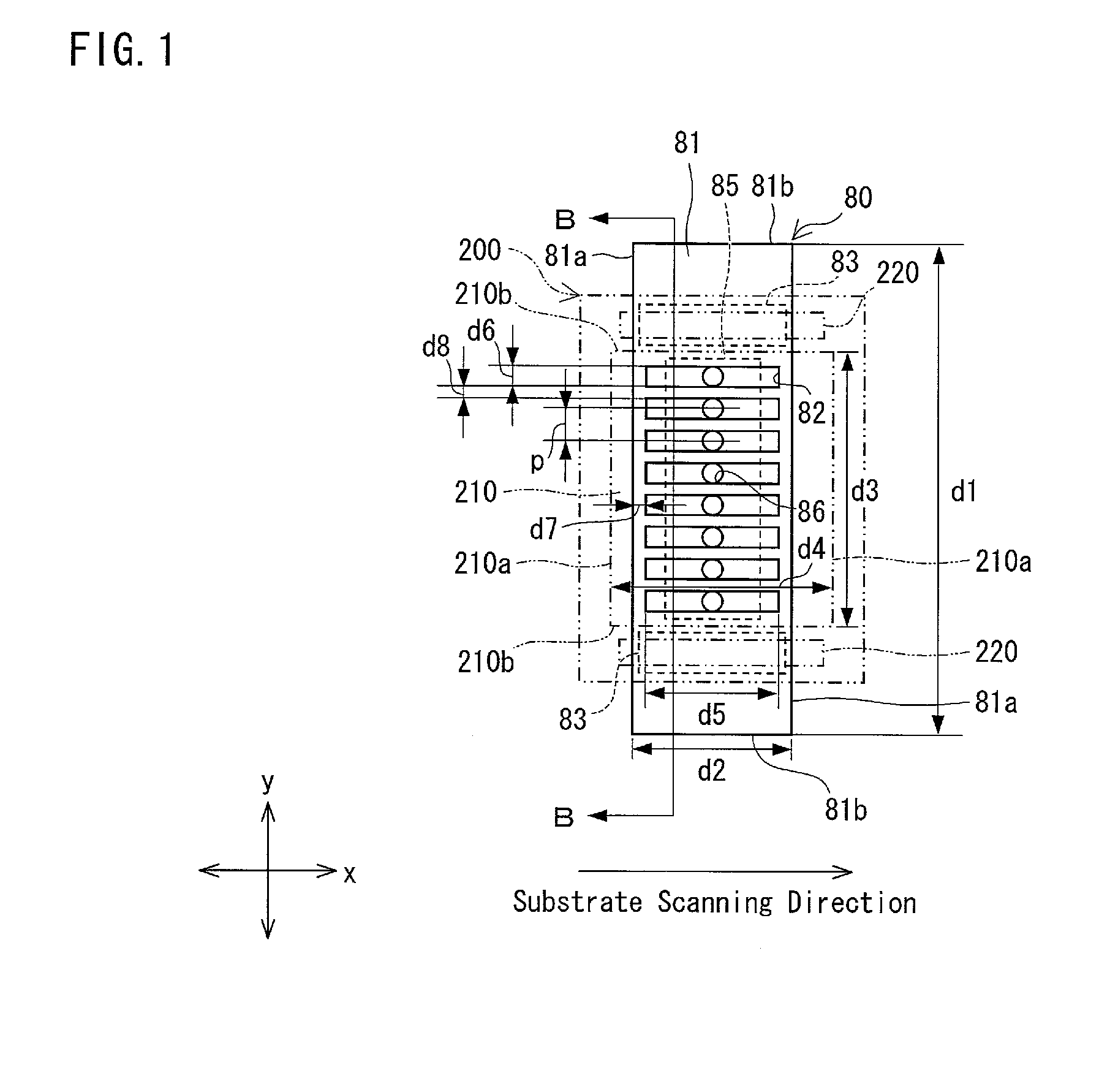
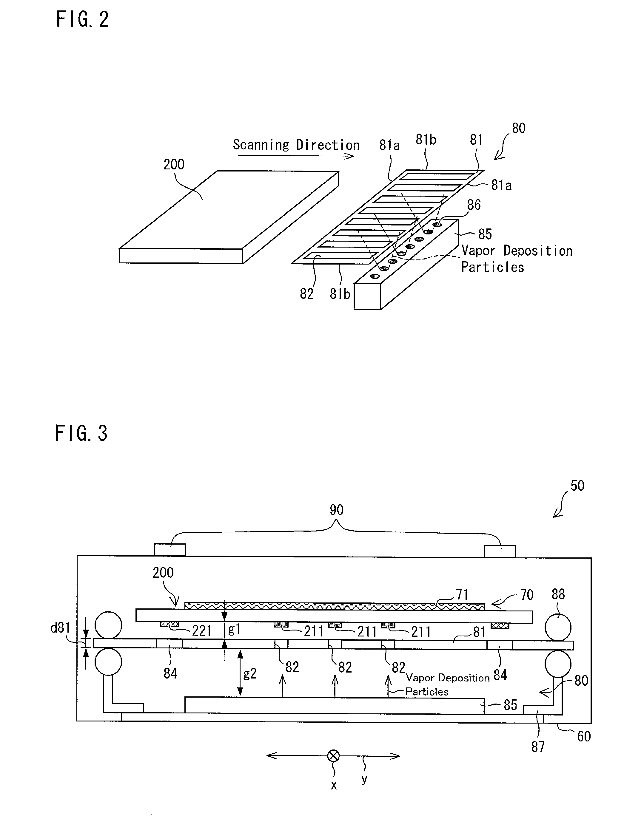
[0080]An embodiment of the present invention is described below with reference to FIGS. 1 through 15.

[0081]The present embodiment describes, as an example vapor deposition method involving a vapor deposition device of the present embodiment, a method for producing an organic EL display device that (i) is of a bottom emission type, that is, extracts light from a TFT substrate side, and that (ii) carries out an RGB full color display.

[0082]The description first deals with the overall configuration of the organic EL display device.

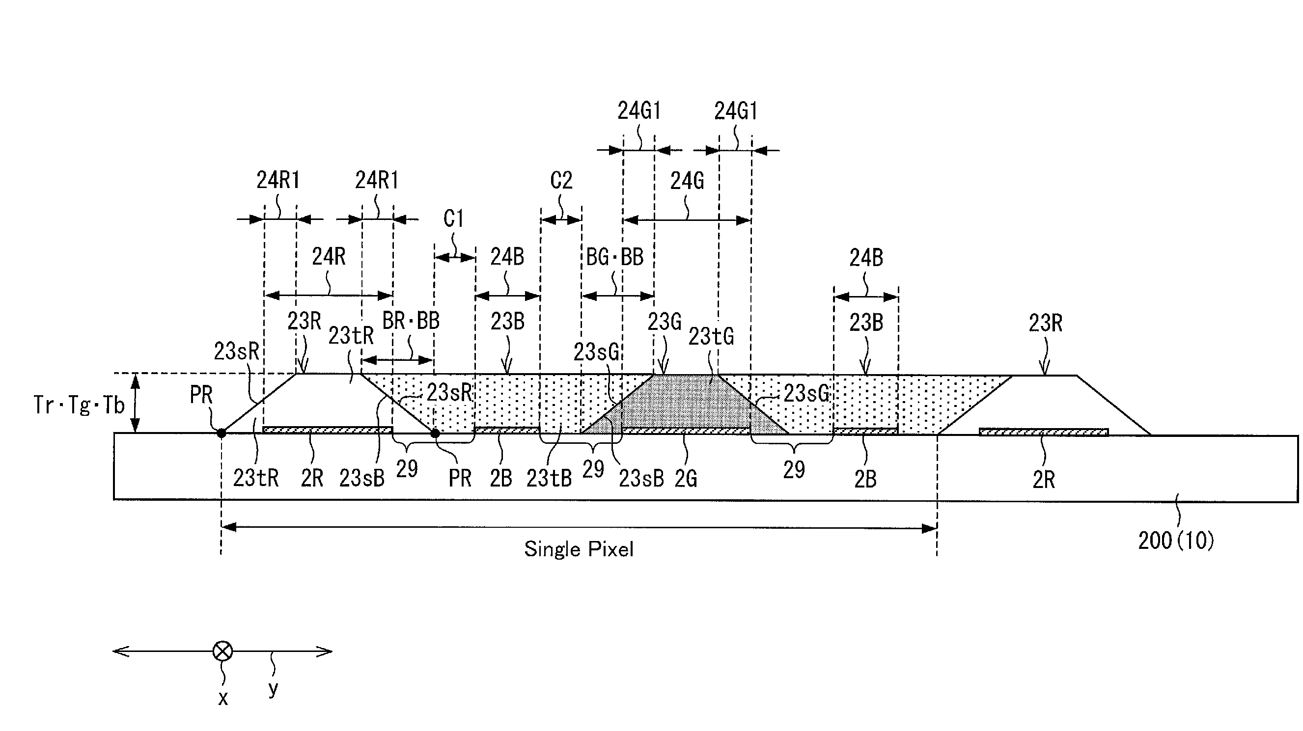
[0083]FIG. 6 is a cross-sectional view schematically illustrating a configuration of the organic EL display device that carries out an RGB full color display. FIG. 7 is a plan view illustrating an arrangement of pixels included in the organic EL display device illustrated in FIG. 6. FIG. 8 is a cross-sectional view, taken long line A-A in FIG. 7, of a TFT substrate included in the organic EL display device illustrated in FIG. 7.

[0084]As illustrated in FIG. 6,...

second embodiment

[0339]With reference to FIG. 16, the following description will discuss another embodiment of the present invention.

[0340]First Embodiment employs an arrangement in which the thicknesses Tr, Tg, and Tb of the substantially flat parts 23tR, 23tG, and 23tB of the luminescent layers 23R, 23G, and 23B are equal to each other. The present embodiment employs an arrangement in which (i) thicknesses Tr and Tg of substantially flat parts 23tR and 23tG of luminescent layers 23R and 23G (first films) are equal to each other but (ii) a thickness Tb of a substantially flat part 23tB of a luminescent layer 23B (a second film) is larger than the thicknesses Tr and Tg of the substantially flat parts 23tR and 23tG of the luminescent layers 23R and 23G (see FIG. 16).

[0341]Further, in the present embodiment, a luminescent layer 23B2 (a third film) having the same color (i.e., blue) as the luminescent layer 23B is provided on each of the luminescent layers 23R and 23G so that film thicknesses in the lu...

third embodiment

[0349]With reference to FIG. 17, the following description will discuss another embodiment of the present invention.

[0350]In Second Embodiment, the thicknesses Tr and Tg of the luminescent layers 23R and 23G, respectively, are equal to each other. In contrast, in the present embodiment, as illustrated in FIG. 17, the thicknesses Tr and Tg of the luminescent layers 23R and 23G (first film) are different from each other.

[0351]In the present embodiment, a luminescent layer 23B2 (hereinafter luminescent layer 23B2R; third film) on the luminescent layer 23R and a luminescent layer 23B2 (hereinafter luminescent layer 23B2G; third film) on the luminescent layer 23G have a substantially flat part 23tB2R with a thickness Tb2r and a substantially flat part 23tB2G with a thickness Tb2r, respectively. The thickness Tb2r of the substantially flat part 23tB2R and the thickness Tb2r of the substantially flat part 23tB2G are represented by equations 6 and 7, respectively.

Tb2r=Tb1−Tr  equation 6

Tb2g...


PUM

PropertyMeasurementUnit
thicknessaaaaaaaaaa
blue luminescentaaaaaaaaaa
sizeaaaaaaaaaa

Abstract

A film formation substrate (200) is arranged such that (i) a base end, in a y-axis direction, of a film-thickness-gradually-diminishing part (23sR) of a first film (23R) overlaps a first film formation region (24R), and (ii) a film-thickness-gradually-diminishing part (23sB) of a second film (23B) is disposed on an outside, in the y-axis direction, of a second film formation region (24B) and overlaps the film-thickness-gradually-diminishing part (23sR) of the first film (23R) so as to compensate for a gradually diminished thickness of the film-thickness-gradually-diminishing part (23sR).

Description

TECHNICAL FIELD[0001]The present invention relates to a film formation substrate that can be employed in an organic EL display device, a method for producing the film formation substrate, and an organic EL display device using the film formation substrate.BACKGROUND ART[0002]Recent years have witnessed practical use of a flat-panel display in various products and fields. This has led to a demand for a flat-panel display that is larger in size, achieves higher image quality, and consumes less power.[0003]Under such circumstances, great attention has been drawn to an organic EL display device that (i) includes an organic electroluminescence (hereinafter abbreviated to “EL”) element which uses EL of an organic material and that (ii) is an all-solid-state flat-panel display which is excellent in, for example, low-voltage driving, high-speed response, and self-emitting.[0004]An organic EL display device includes, for example, (i) a substrate made up of members such as a glass substrate a...

Claims


Application Information

Patent Timeline
Patent Type & Authority Applications(United States)
IPC IPC(8): H05B33/14
CPCH05B33/145C23C14/042C23C14/54Y10T428/24612H10K59/35H10K59/12H10K71/10H10K71/00H10K2102/351H10K50/125
Inventor SONODA, TOHRUKAWATO, SHINICHIINOUE, SATOSHIHASHIMOTO
Owner SHARP KK
Why Eureka
Try Eureka