Light-emitting device

a light-emitting device and light-emitting technology, which is applied in the direction of static indicating devices, solid-state devices, instruments, etc., can solve the problems of large load on the signal line driver circuit, high production cost of ic chips of light-emitting devices, and low market penetration rate of light-emitting devices

Inactive Publication Date: 2013-12-05
SEMICON ENERGY LAB CO LTD
View PDF2 Cites 10 Cited by
  • Summary
  • Abstract
  • Description
  • Claims
  • Application Information

AI Technical Summary

Benefits of technology

[0017]In one embodiment of the present invention, it is possible to provide a light-emitt

Problems solved by technology

The light-emitting devices are putting into practical use; however, the market penetration rate of the light-emitting devices is much lower than that of liquid crystal display devices.
Consequently, the production cost of the IC chips of the light-emitting devices is high.
Consequently, drive frequency needed for the signal line driver circuit for the liquid crystal display device is approximately twice that of the signal line driver circuit for the light-emitting devi

Method used


Image

  • Light-emitting device
  • Light-emitting device
  • Light-emitting device

Examples


embodiment 1

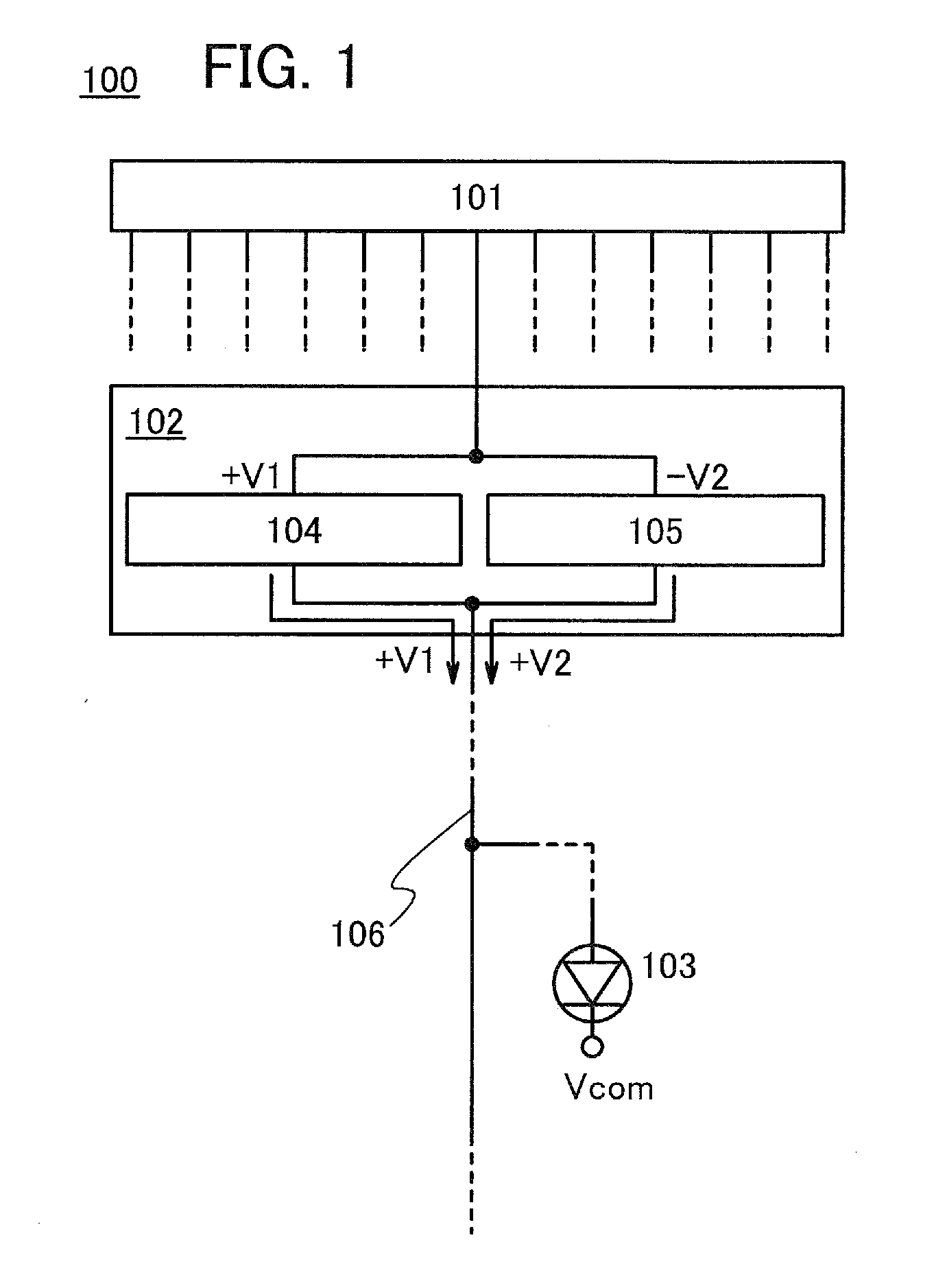
[0034]FIG. 1 illustrates a structure example of a light-emitting device 100 according to one embodiment of the present invention. The light-emitting device 100 in FIG. 1 includes a signal line driver circuit 101 generating a first image signal having a positive polarity and a second image signal having a negative polarity, a selection circuit 102 holding the first image signal having a positive polarity and the second image signal having a negative polarity and making the two image signals have the same polarity by converting the polarity of one of the two held image signals into an opposite polarity, and a light-emitting element 103 whose luminance is sequentially determined in response to the two image signals.

[0035]Specifically, the signal line driver circuit 101 has a function of converting an input serial image signal into a parallel image signal and outputting the parallel image signal. Further, among image signals output from the signal line driver circuit 101, one of a first...

embodiment 2

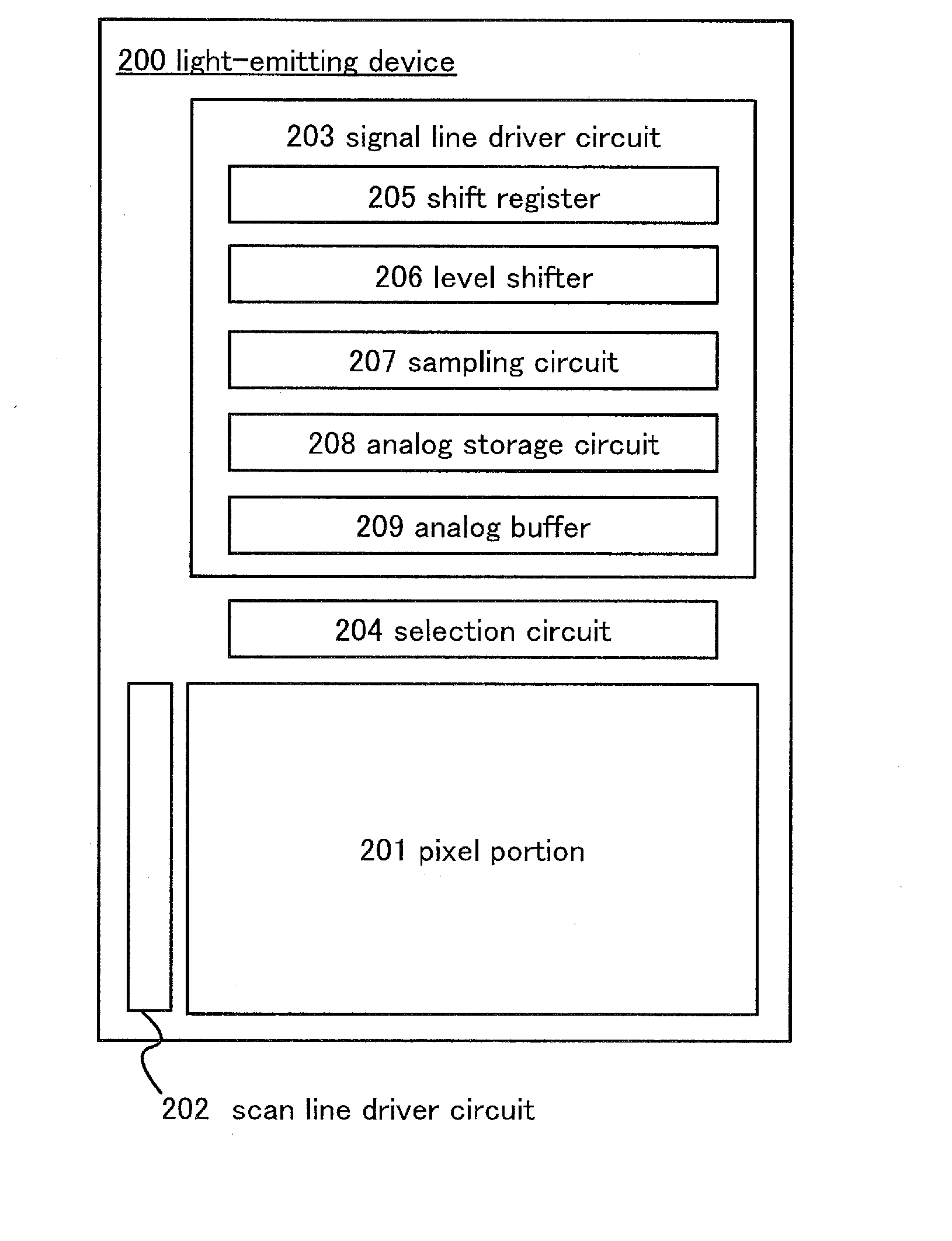
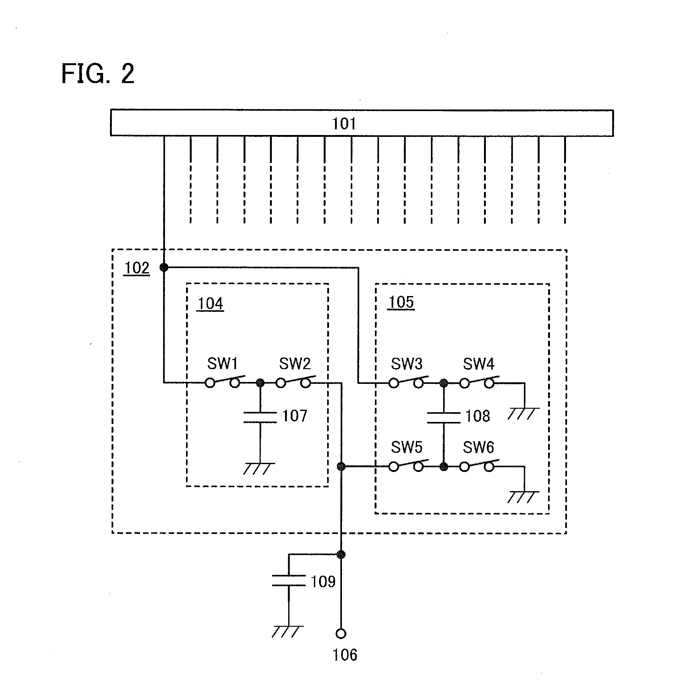
[0077]FIG. 7 is a block diagram illustrating a structure example of a light-emitting device according to one embodiment of the present invention. A light-emitting device 200 in FIG. 7 includes a pixel portion 201 in which a light-emitting element is provided in each pixel, and driver circuits controlling the operation of the pixel portion 201. The light-emitting device 200 in FIG. 7 includes a scan line driver circuit 202, a signal line driver circuit 203, and a selection circuit 204 as the driver circuits.

[0078]The scan line driver circuit 202 has a function of selecting pixels included in the pixel portion 201. The signal line driver circuit 203 has a function of outputting an image signal having a positive polarity and an image signal having a negative polarity that correspond to pixels selected by the scan line driver circuit 202. The selection circuit 204 has a function of inverting the polarity of one of the image signal having a positive polarity and the image signal having a...

embodiment 3

[0097]In this embodiment, a specific structure example of a pixel of a light-emitting device according to one embodiment of the present invention is described. Note that a transistor in the pixel corresponds to a semiconductor element in one embodiment of the present invention.

[0098]FIG. 8A shows an example of a circuit diagram of a pixel 300. The pixel 300 includes a transistor 301 controlling input of an image signal to the pixel 300, a light-emitting element 302, a transistor 303 controlling the value of current supplied to the light-emitting element 302 in response to an image signal, and a capacitor 304 for holding the potential of an image signal.

[0099]The potential of one of an anode and a cathode of the light-emitting element 302 is controlled in response to an image signal input to the pixel 300. The reference potential Vcom is applied to the other of the anode and the cathode of the light-emitting element 302. The luminance of the light-emitting element 302 is determined b...


PUM


Abstract

A light-emitting device capable of displaying an image using image signals having different polarities is provided. The light-emitting device includes a first circuit holding a first image signal having a first polarity, a second circuit holding a second image signal having a second polarity different from the first polarity and converting the second polarity of the held second image signal into the first polarity, and a light-emitting element whose luminance is sequentially determined in response to the first image signal held in the first circuit and the second image signal whose polarity is converted into the first polarity in the second circuit.

Description

BACKGROUND OF THE INVENTION[0001]1. Field of the Invention[0002]The present invention relates to a light-emitting device in which a light-emitting element is provided in each pixel.[0003]2. Description of the Related Art[0004]The number of pixels in a semiconductor display device such as a liquid crystal display device or a light-emitting device has been increased to display images with higher definition and higher resolution. Thus, a scan line driver circuit and a signal line driver circuit need to be driven at high speed. In particular, while pixels in lines are selected by the scan line driver circuit, the signal line driver circuit needs to input image signals to all the pixels in the lines. Thus, the drive frequency of the signal line driver circuit is much higher than that of the scan line driver circuit.[0005]In order to achieve driving at high drive frequency, it is effective to use a transistor having high mobility and a channel formation region including crystalline silico...

Claims


Application Information

Patent Timeline
IPC IPC(8): H01L27/15G09G3/20
CPCH01L27/15G09G3/20G09G3/3233G09G3/3614G09G3/3688G09G2310/0291
Inventor KOYAMA, JUN
Owner SEMICON ENERGY LAB CO LTD
Why Eureka
Try Eureka