
Field effect transistor, display device , sensor, and method of manufacturing field effect transistor

Active Publication Date: 2013-12-12
SAMSUNG DISPLAY CO LTD
View PDF2 Cites 7 Cited by
  • Summary
  • Abstract
  • Description
  • Claims
  • Application Information

AI Technical Summary

Benefits of technology

The invention provides a field effect transistor (FET) that has improved mobility while using an oxide semiconductor structure containing main elements of Sn, Zn, and O or Sn, Ga, Zn, and O. This FET can be used in display devices, sensors, and other applications. The technical effect of this invention is to improve the performance and efficiency of the FET, which can lead to better functionality and performance of the overall device.

Problems solved by technology

However, in order to fabricate a TFT that is IGZO and has high mobility, post-annealing at a high temperature (e.g., greater than or equal to 400° C. in the atmosphere) is needed, and it is difficult to form TFTs on flexible substrates that have low heat-resistance.

Method used


Image

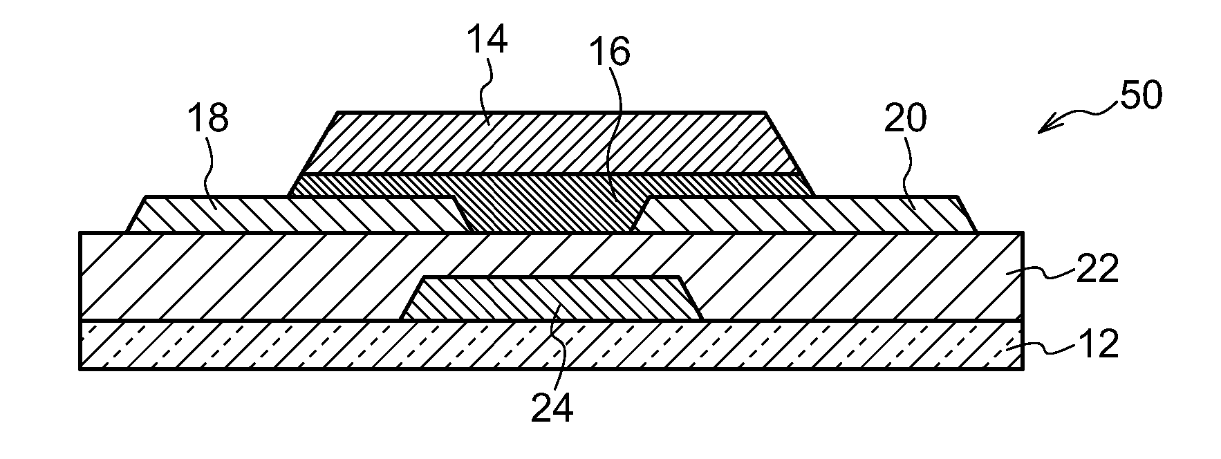
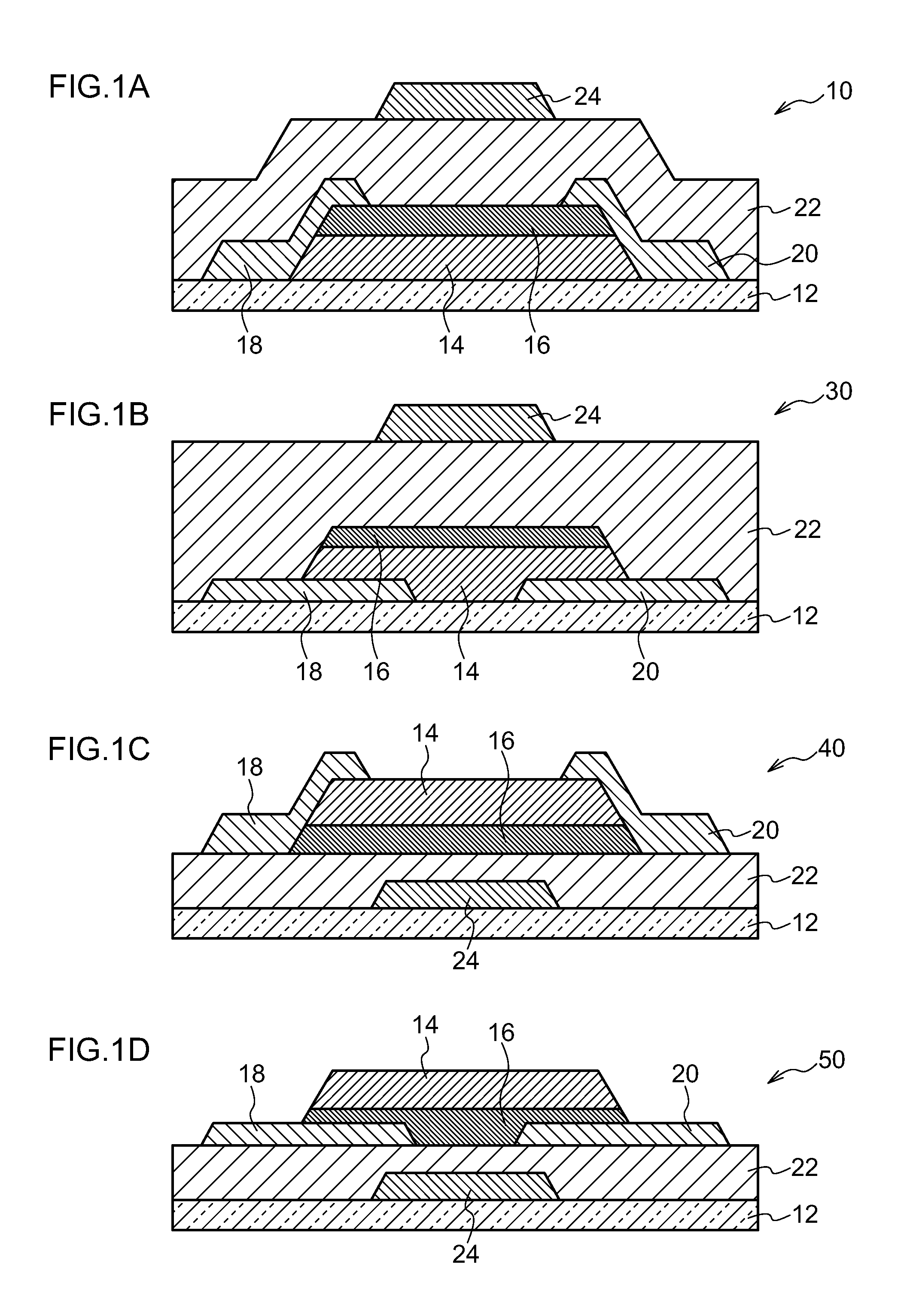
  • Field effect transistor, display device , sensor, and method of manufacturing field effect transistor
  • Field effect transistor, display device , sensor, and method of manufacturing field effect transistor
  • Field effect transistor, display device , sensor, and method of manufacturing field effect transistor

Examples


examples

[0144]Examples are described hereinafter, but the present invention is not limited in any way by these Examples.

[0145]TFT characteristic evaluation was carried out on TFTs that used, as an oxide semiconductor layer, an SGZO film whose main structural elements were Sn, Zn and O, or Sn, Ga, Zn and O, while changing the absence / presence of an oxide intermediate layer and the type of the oxide intermediate layer. FIG. 8A is a plan view of the TFTs of the Examples and Comparative Examples, and FIG. 8B is a sectional view along arrow A-A of the TFT shown in FIG. 8A.

[0146]As shown in FIG. 8A and FIG. 8B, in Examples 1 through 4, a simple TFT 500 was fabricated by using, as the substrate, a p-type Si substrate 502 (1 inch square×1 mmt, thickness: 525 μmt, thermal oxidation film (SiO2): 100 nmt) having a thermal oxidation film 504, and by using the thermal oxidation film 504 as a gate insulating film.

[0147]Concretely, an oxidation intermediate layer 506 was film-formed by sputtering to a thi...


PUM


Abstract

A field effect transistor including: a gate insulating film; an oxide semiconductor layer that serves as an active layer and whose main structural elements are Sn, Zn and O, or Sn, Ga, Zn and O; and an oxide intermediate layer that is disposed between the gate insulating film and the oxide semiconductor layer, and whose resistivity is higher than that of the oxide semiconductor layer.

Description

CROSS-REFERENCE TO RELATED APPLICATIONS[0001]This application is a continuation application of International Application No. PCT / JP2012 / 054006, filed Feb. 20, 2012, the disclosure of which is incorporated herein by reference in its entirety. Further, this application claims priority from Japanese Patent Application No. 2011-055559, filed Mar. 14, 2011, the disclosure of which is incorporated herein by reference in its entirety.BACKGROUND[0002]1. Technical Field[0003]The present invention relates to a field effect transistor, a display device, a sensor, and a method of fabricating a field effect transistor.[0004]2. Related Art[0005]Field effect transistors are widely used as unit elements of integrated circuits for semiconductor memories, high-frequency signal amplifying elements, elements for driving display elements such as liquid crystals, and the like. Field effect transistors that are made to be thin-filmed in particular are called thin film transistors (TFTs). Further, a silico...

Claims


Application Information

Patent Timeline
IPC IPC(8): H01L29/786H01L29/66
CPCH01L29/7869H01L29/66969G02F1/1368H01L29/78696H01L27/14658G02F1/13685H10K59/1213H01L27/144H01L29/78606H01L29/78693
Inventor TAKATA, MASAHIROTANAKA, ATSUSHI
Owner SAMSUNG DISPLAY CO LTD
Learn More