

Method of semiconductor film stabilization
a technology of film stabilization and semiconductor, applied in the direction of crystal growth process, polycrystalline material growth, after-treatment details, etc., can solve the problems of less resistivity and threshold voltage, less electronic properties of channel, and large size of transistor components
- Summary
- Abstract
- Description
- Claims
- Application Information
AI Technical Summary
Benefits of technology
Problems solved by technology
Method used
Image

Examples
Embodiment Construction
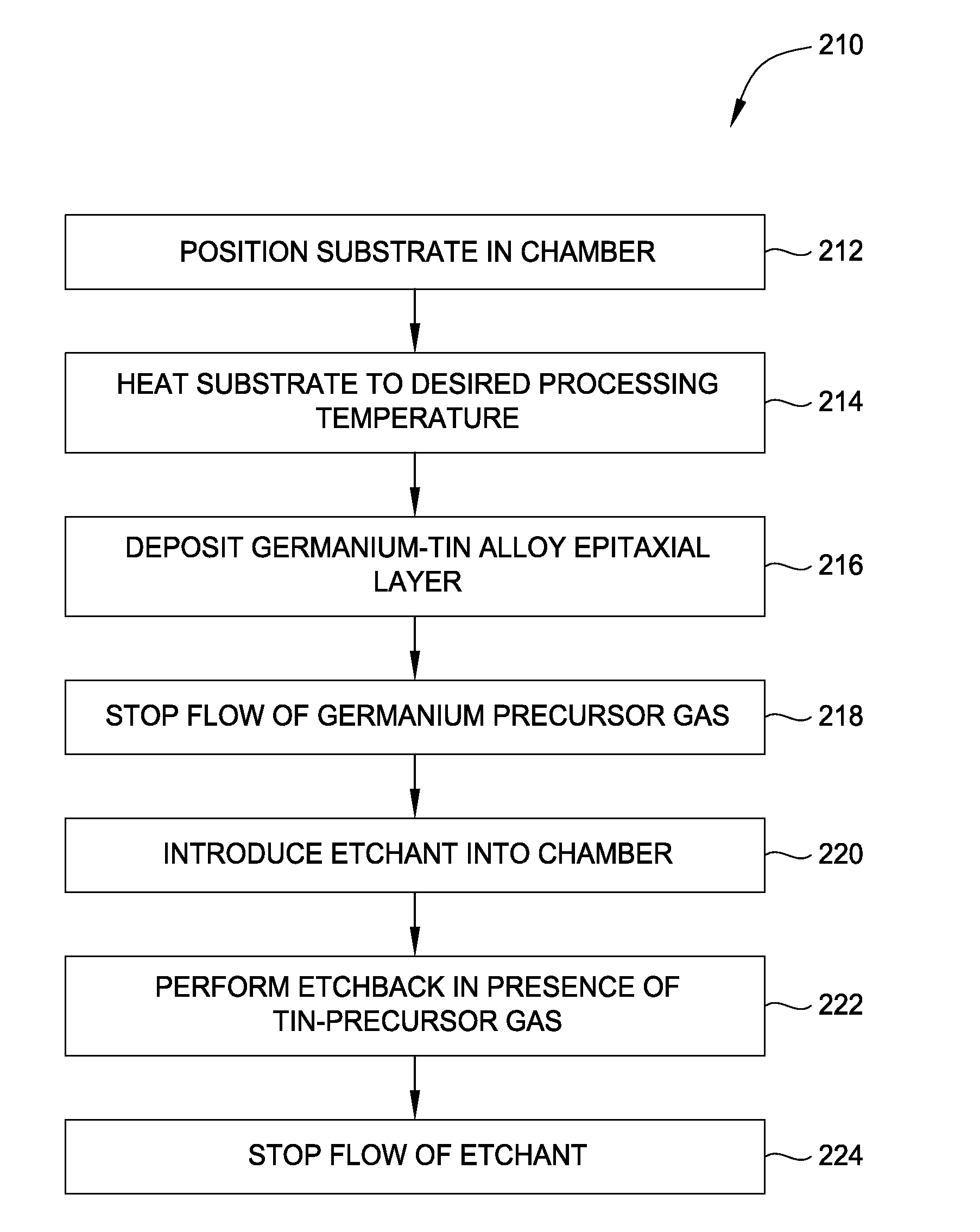
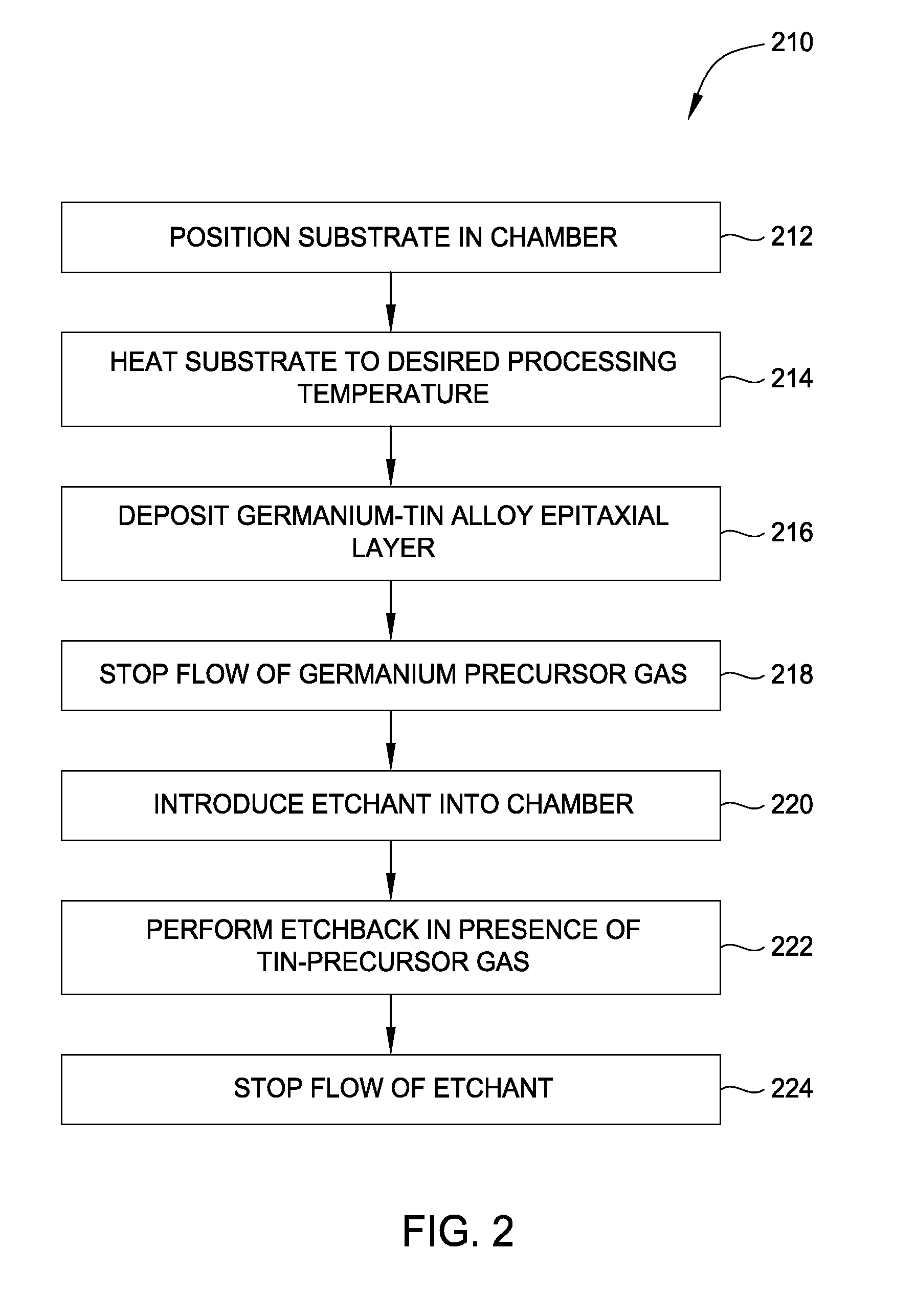
[0015]Embodiments of the invention generally relate to methods for forming silicon-germanium-tin alloy epitaxial layers, germanium-tin alloy epitaxial layers, and germanium epitaxial layers that may be doped with boron, phosphorus, arsenic, or other n-type or p-type dopants. The methods generally include positioning a substrate in a processing chamber. A germanium precursor gas, and optionally a silicon precursor gas and a group III or group V gas, is then introduced into the chamber concurrently with an alloying precursor gas, such as a tin precursor gas, to form an epitaxial layer. The flow of the germanium gas is then halted, and an etchant gas is introduced into the chamber. An etch back is then performed while in the presence of the alloying precursor gas used in the formation of the epitaxial film. The flow of the etchant gas is then stopped, and the cycle may then be repeated. In addition to or as an alternative to the etch back process, an annealing processing may be perform...
PUM
 Abstract
Description
Claims
Application Information