
Method for Forming Silicon-Containing Dielectric Film by Cyclic Deposition with Side Wall Coverage Control

a dielectric film and cyclic deposition technology, applied in chemical vapor deposition coating, coating, metallic material coating process, etc., can solve the problems of thin deterioration of film deposited on a sidewall, and low sidewall reaction rate of nitration

Active Publication Date: 2013-12-12
ASM IP HLDG BV
View PDF2 Cites 372 Cited by
  • Summary
  • Abstract
  • Description
  • Claims
  • Application Information

AI Technical Summary

Benefits of technology

The present invention provides a method for forming a dielectric film with Si-C bonds and / or Si-N bonds on a semiconductor substrate through cyclic deposition. The method includes conducting one or more cycles of cyclic deposition using a Si-containing precursor and a reactant gas, followed by applying a pulse of RF power to the reaction space while supplying a rare gas and a treatment gas without supplying a Si-containing precursor. The resulting dielectric film formed on the substrate has Si-C bonds and / or Si-N bonds. The method also includes determining the side wall coverage of the first dielectric film and conducting steps to form a second dielectric film with higher side wall coverage than the first film. Overall, this method provides a reliable and effective way to form dielectric films with specific bond types on semiconductor substrates.

Problems solved by technology

This problem may be caused by ion collision interfering with reaction speed on the sidewall as compared with that on a top or bottom surface.
Particularly, nitration has a low rate of sidewall reaction as compared with oxidation, causing problems of thin film deposited on a sidewall, deterioration of film deposited on a sidewall, etc.

Method used


Image

  • Method for Forming Silicon-Containing Dielectric Film by Cyclic Deposition with Side Wall Coverage Control
  • Method for Forming Silicon-Containing Dielectric Film by Cyclic Deposition with Side Wall Coverage Control
  • Method for Forming Silicon-Containing Dielectric Film by Cyclic Deposition with Side Wall Coverage Control

Examples


example 8

[0130]Precursor: Tetrachlorodimethylsilane

[0131]Precursor inflow pressure: 66.6 Pa

[0132]Substrate temperature: 400° C.

[0133]Carrier gas flow: Ar at 2 SLM

[0134]Reactant gas flow: H2 at 0.5 SLM

[0135]RF frequency: 13.56 MHz

[0136]RF power: 400 W

[0137]Precursor supply time (steps 1a+2a): 2 seconds

[0138]RF Plasma exciting time (step 2a): 1.3 seconds

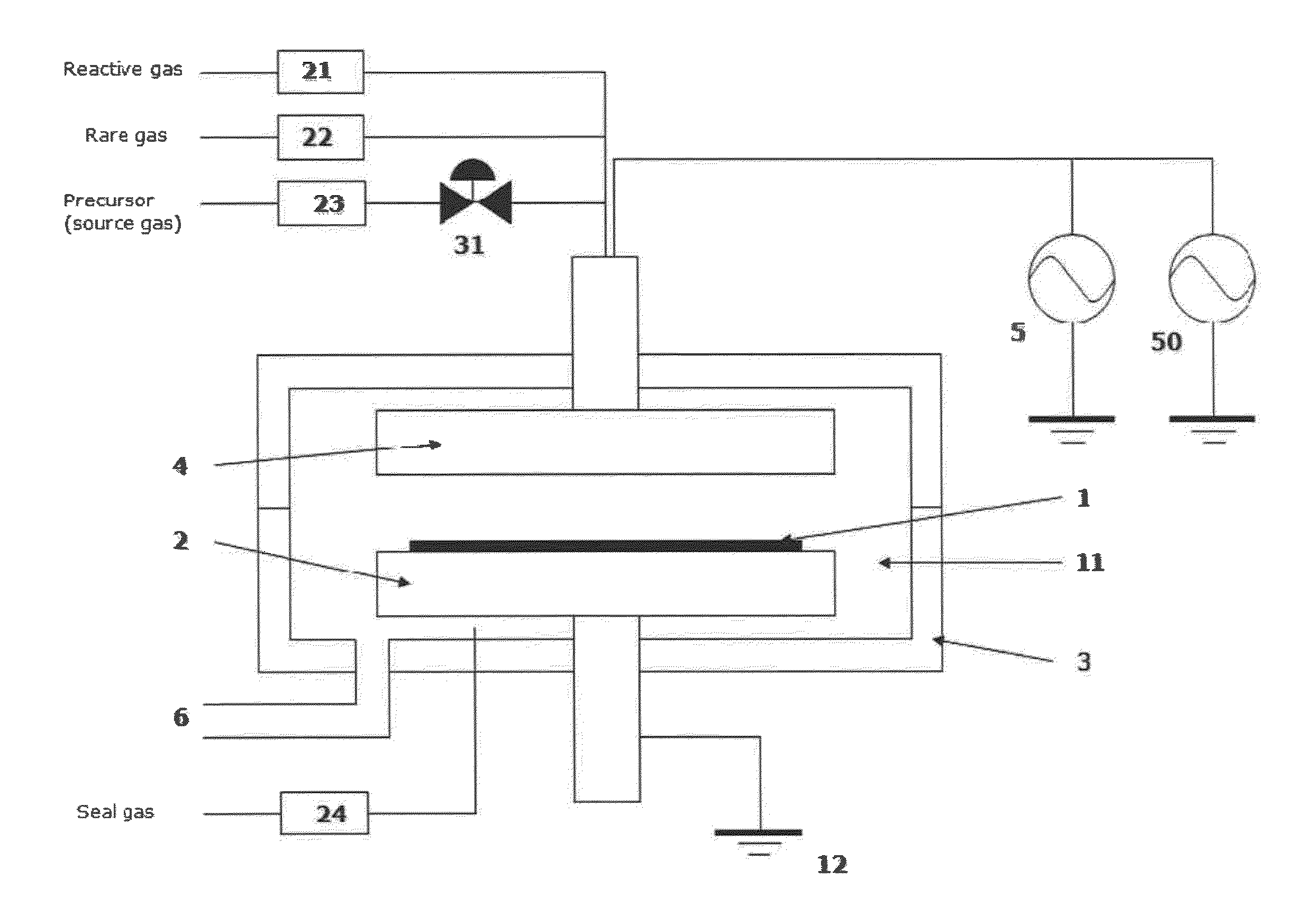
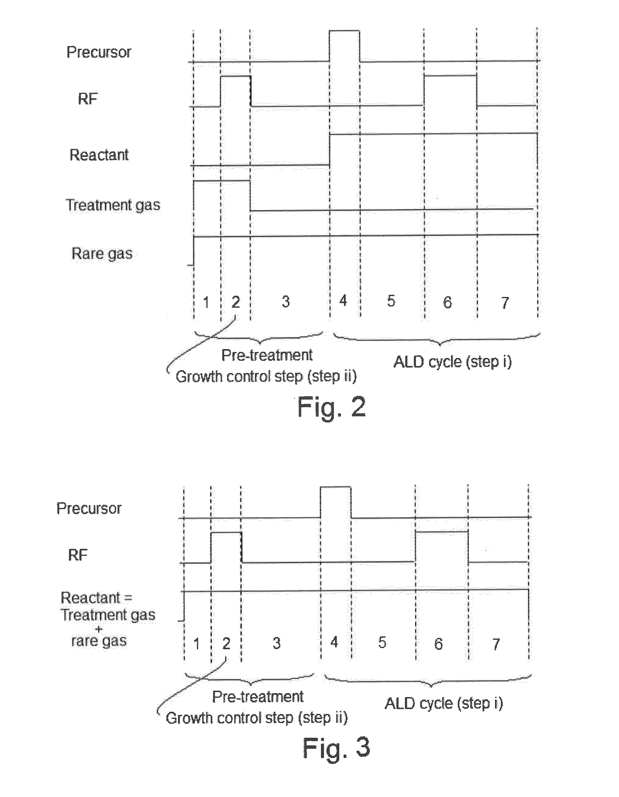
[0139]The growth control step (step 2 in FIG. 2; step 3a in FIG. 5) was performed under conditions shown in Table 1. Incidentally, the duration of step 1 in FIG. 2 was 0.5 seconds, and the duration of step 3 in FIG. 2 was 0.5 seconds.

TABLE 1CyclesperTotalgrowthdepositionTem.TreatmentRareRFDurationPressurecontrolcyclesFilm(° C.)gasgas(W)(sec)(Pa)(N)(M · N)Com 1SiN400500Ex 1SiN400H2:He:500604005005001SLM1SLMEx 2SiN400H2:He:5000.140015001SLM1SLMCom 2SiC400500Ex 3SiC100H2:He:500603005005000.5SLM1SLMEx 4SiC100H2:He:5000.230015000.5SLM1SLMEx 5SiC400NH3:He:400604005005001SLM1SLMEx 6SiC400NH3:He:4000.140015001SLM1SLMEx 7SiC400CH4He:400604005005000.01SL...


PUM

PropertyMeasurementUnit
Temperatureaaaaaaaaaa
Fractionaaaaaaaaaa

Abstract

A method of forming a dielectric film having Si—C bonds and / or Si—N bonds on a semiconductor substrate by cyclic deposition, includes: (i) conducting one or more cycles of cyclic deposition in a reaction space wherein a semiconductor substrate is placed, using a Si-containing precursor and a reactant gas; and (ii) before or after step (i), applying a pulse of RF power to the reaction space while supplying a rare gas and a treatment gas without supplying a Si-containing precursor, whereby a dielectric film having Si—C bonds and / or Si—N bonds is formed on the semiconductor substrate.

Description

BACKGROUND[0001]1. Field of the Invention[0002]The present invention relates generally to semiconductor integrated circuit manufacturing and, more particularly to a method of forming a silicon-containing dielectric film on a semiconductor substrate by cyclic deposition such as atomic layer deposition and cyclic chemical vapor deposition with side wall coverage control.[0003]2. Description of the Related Art[0004]As methods of depositing dielectric films on substrates, typically chemical vapor deposition (CVD) and atomic layer deposition (ALD) are known. A skilled artisan often uses plasma-enhanced CVD (PE-CVD) and plasma-enhanced ALD (PE-ALD) to form dielectric films. PE-ALD is a deposition technology of dielectric films using chemisorption of precursors and can improve a step coverage of films depositing on recess patterns of substrates, as compared with PE-CVD. However, when depositing a dielectric film other than SiO film by PE-ALD on a recess pattern, where nitration or carbon s...

Claims


Application Information

Patent Timeline
IPC IPC(8): H01L21/31
CPCC23C16/325C23C16/345C23C16/45536H01L21/02167H01L21/0217H01L21/02211H01L21/02274H01L21/0228
Inventor FUKAZAWA, ATSUKIOKA, TAKAHIRO
Owner ASM IP HLDG BV
Learn More