

Method for reclaiming wafer substrate and polishing solution compositions therefor
a technology of wafer substrate and polishing solution, which is applied in the direction of basic electric elements, semiconductor/solid-state device manufacturing, electric apparatus, etc., can solve the problems of high cost of test grade wafers compared to general test grade wafers, ineffective uniform reclamation of large wafers, and ineffective etching process of chemical etching process, etc., to achieve the effect of polishing silicon wafers and increasing the number of times a wafer substrate is recycled
- Summary
- Abstract
- Description
- Claims
- Application Information
AI Technical Summary
Benefits of technology
Problems solved by technology
Method used
Image

Examples
example 1
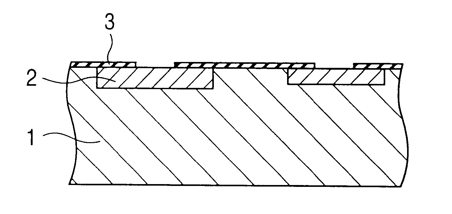
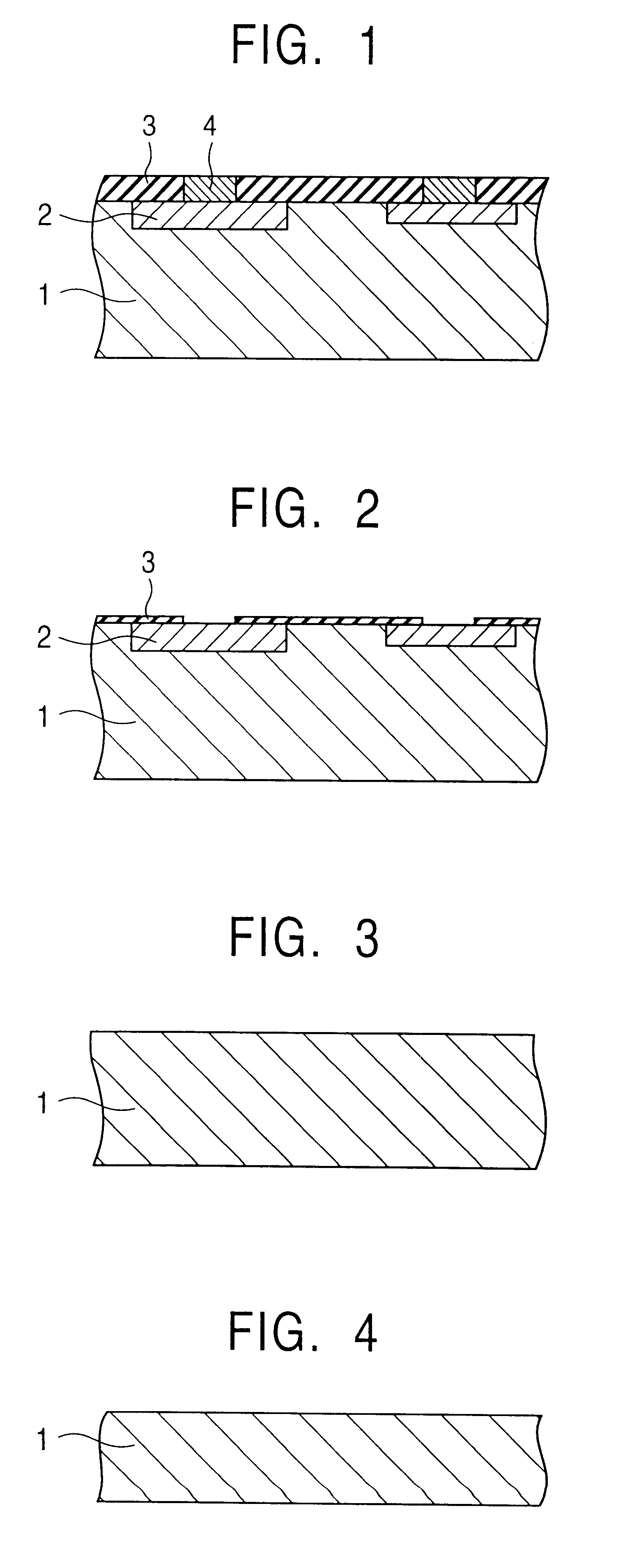
A nitride or oxide surface layer shown in Table 2 was formed on the front surface of an 8-inch single crystal wafer substrate having a thickness of 725 .mu.m and a {100} plane crystal orientation. Six substrates for each surface layer (twelve substrates in total) were prepared and used for reclamation treatment.
An etching solution of 69% nitric acid:49% hydrofluoric acid:pure water=1:1:5 (by volume) was poured into a Teflon bath, and then used wafers having the layer configurations shown in Table 2 were immersed therein and were subjected to etching at room temperature for 5 minutes. Most parts of the group 1 wafers became colored during the etching to greenish to reddish in response to the thickness of the nitride film which remained on the wafer. The center of the group 2 wafers became colored by the etching to yellowish to bluish due to the residual oxide film, although the aluminum layer was completely removed.
After this metal layer was removed by etching the following surface f...
example 2
A nitride or oxide surface layer shown in Table 2 was formed on the front surface of an 8-inch single crystal wafer substrate having a thickness of 725 .mu.m and a {100} plane crystal orientation. Six substrates for each surface layer (twelve substrates in total) were prepared and used for reclamation treatment. An etching solution composed of an aqueous 25% sodium peroxodisulfate solution:concentrated sulfuric acid (96%)=1:1 (by volume) was poured into a quartz bath, and then used wafers having the layer configurations shown in Table 2 were immersed therein and were subjected to etching at 100.degree. C. for 10 minutes. Next, the wafers were immersed into a Teflon bath containing an etching solution of 49% hydrofluoric acid:water=1:2 (by volume) at room temperature for 10 minutes.
The group 1 wafers changed color during the etching, but films remained on the entire surface. In the group 1 wafers, a yellowish to bluish part due to the residual oxide film remained in the center, altho...
PUM
 Abstract
Description
Claims
Application Information