Combined metallic bonding and molding for electronic assemblies including void-reduced underfill

a technology of electronic assemblies and metallic bonding, which is applied in the direction of manufacturing tools, mold control devices, and foundation moulding apparatus, etc., can solve the problems of significant density of underfill voids, loss of reliability, and various components contracting at different rates during bonding, so as to reduce voids and/or the size of voids, and reduce joint misalignment

Active Publication Date: 2009-11-26
TEXAS INSTR INC
View PDF5 Cites 49 Cited by
  • Summary
  • Abstract
  • Description
  • Claims
  • Application Information

AI Technical Summary

Benefits of technology

[0012]The vacuum applied during the placing / first bonding has been found by the Present Inventor to significantly reduce voiding and / or the size of the voids in the underfill as compared to convention TCB processing. Other embodiments of the invention describe new pressing systems and related methods that form a closed volume around the IC die when the workpiece comprises a package substrate and a substantially closed volume in the case the workpiece comprises a wafer, which has been found by the Present Inventor to further reduce underfill voiding and / o the size of the voids.
[0013]Embodiments of the invention are also described for reducing joint misalignment. Embodiments of the invention include presses that unlike conventional clam-shell based pressing equipment do not pivot around a hinge, that press with a nearly 90° force to simultaneously push the plurality of ICs to reduce joint misalignment. Particularly for package substrate applications, the pressing can utilize a pressing system comprising a first pressing head for pressing each of the plurality of IC die and an independently movable second pressing head for pressing the package substrate surface beyond the IC die to help keep the package substrate from bowing (expanding) during pressing, wherein the first pressing head initially contacts the plurality of IC die at a maximum tilt angle of 0.2 degrees. Separate pressing heads allow a different force / area (pressure) to be applied to the substrate as compared to the force / area applied to the IC die, as well as the pressing heads to contact at different times.
[0014]Moreover, embodiments of the invention generally provide high throughput. One aspect of embodiments of the invention that provides high throughput is the curing of the curable dielectric film during pressing, thus eliminating the need for a separate curing step.

Problems solved by technology

Injection of underfill is known to result in a significant density of underfill voids, particularly when the geometries (e.g., of the gaps) to be filled are relatively small.
Voids typically result in a loss of reliability.
Moreover, a drawback with soldering the IC die to the substrate is that the various components contract at different rates during bonding.
However, TCB like conventional wafer scale bonding, is known to result in generation of a significant density of reliability reducing underfill voids, many of which can be of significant size.
The Present Inventor has recognized that conventional microelectronic assembly processes that include forming metallic joints generally have one or more problems, including throughput / cost, underfill voiding, and misaligned joints.
Although TCB as described above generally provides high throughput and thus low cost, TCB generally results in a significant density of underfill voids, which can also be of significant size.
Capillary underfill may reduce the density and size of underfill voids compared to PCB, but as the size of the gap to be filled is reduced, as is the current trend, the height of the gap for injection may not be enough and result in incomplete filling.
Regarding misalignment of joints, the Present Inventor has recognized a problem with pressing using conventional clam-shell based pressing equipment is that the clamming motion, which pivots around a hinge, necessarily causes the respective clam shells of the clam to meet at an angle other than 90 degrees during pressing, and thus imparts a lateral (horizontal) force on the IC die relative to the wafer or package substrate surface.
Even though the deviation from 90 degrees (vertical) may be small, the deviation can be sufficient to shift the IC die relative to the wafer or package substrate surface to result in misaligned joints.
Misaligned joints can result in high resistance joints, or even open circuits, as well as reduced reliability.
Without the substrate held, after IC die is held by inner pressing tool 231, free expansion of the package substrate could result in bump or other bonding conductor slippage.

Method used


Image

  • Combined metallic bonding and molding for electronic assemblies including void-reduced underfill
  • Combined metallic bonding and molding for electronic assemblies including void-reduced underfill
  • Combined metallic bonding and molding for electronic assemblies including void-reduced underfill

Examples


example

[0067]Embodiments of the present invention are further illustrated by the following specific Examples, which should not be construed as limiting the scope or content of embodiments of the invention in any way.

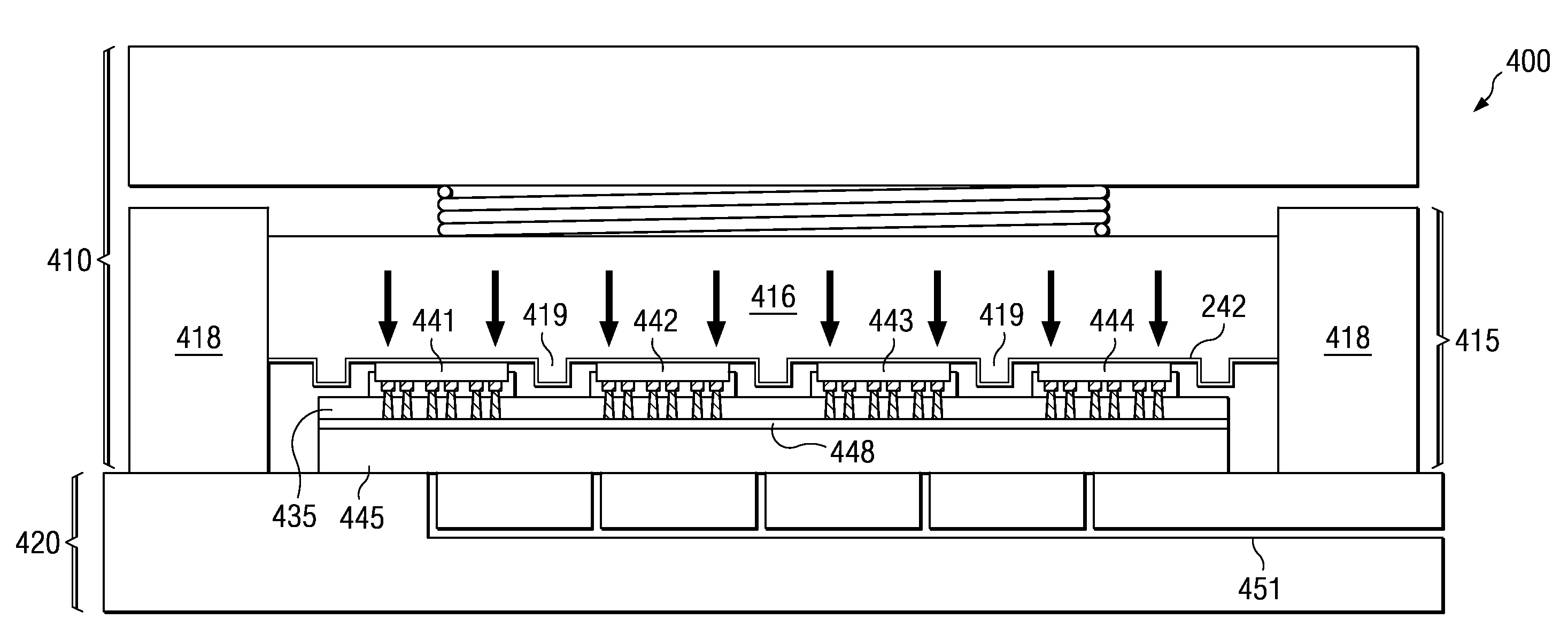
[0068]A series of experiments were performed to determine the effectiveness on underfill voiding by applying vacuum or no vacuum in combinations of the first and second bonding. The workpiece included solder bumps on copper land pads. It was found that air should be removed to <1 kPa (<7.5 torr) during the first bonding to obtain minimum voiding. Vacuum during the second bonding did not measurably reduce bonding as compared to using no vacuum for both the first and second bonding. It was concluded that once air remains in the layers through the first bonding, it did not remove upon the second bonding even with a vacuum. Significantly, if the first bonding is performed under vacuum, there is generally no advantage to second bonding with a vacuum. Void data obtained from the expe...


PUM

PropertyMeasurementUnit
pressureaaaaaaaaaa
pressureaaaaaaaaaa
tilt angleaaaaaaaaaa

Abstract

A method for forming electronic assemblies includes providing a plurality of IC die each having IC bonding conductors and a workpiece having workpiece bonding conductors. A curable dielectric film is applied to the IC bonding conductors or the workpiece surface. The plurality of IC die are placed on the workpiece surface so that the plurality of IC bonding conductors are aligned to and face the plurality of workpiece bonding conductors to provide a first bonding. The placing is performed at a vacuum level corresponding to a pressure <1 kPa, and at a temperature sufficient to provide tackiness to the curable dielectric film. The plurality of IC die are then pressed to provide a second bonding. A temperature during pressing cures the curable dielectric film to provide an underfill and forms metallic joints between the plurality of IC bonding conductors and the plurality of workpiece bonding conductors.

Description

CROSS REFERENCE TO RELATED APPLICATIONS[0001]This application claims the benefit of Provisional Application Ser. No. 61 / 055,289 entitled “P3 (Pick up, Plane and Press) Bond for Flip Chip and Silicon Through Hole Joint,” filed May 22, 2008, which is herein incorporated by reference in its entirety.FIELD OF THE INVENTION[0002]Embodiments of the present invention generally relate to integrated circuit (IC) assembly manufacturing processes and more particularly to IC-to-package substrate or IC-to-wafer assembly and electronic assemblies therefrom.BACKGROUND[0003]Flip-chip technology has recently moved from a specialized packaging application to mainstream production as an important method for improving circuit densities, reliability and cost in miniaturized electronic products. The use of an underfill encapsulant beneath the flip-chip die is generally necessary to improve reliability by reducing the strain on the solder bumps during thermal cycling imposed by coefficient of thermal expa...

Claims


Application Information

Patent Timeline
Patent Type & Authority Applications(United States)
IPC IPC(8): H01L21/50B22D2/00H01L21/60
CPCH01L21/56H01L24/13H01L24/16H01L24/29H01L24/32H01L24/75H01L24/81H01L24/83H01L24/92H01L24/94H01L24/97H01L25/0657H01L25/50H01L2224/1134H01L2224/13009H01L2224/131H01L2224/13144H01L2224/13147H01L2224/16225H01L2224/73204H01L2224/75H01L2224/753H01L2224/75303H01L2224/75314H01L2224/75315H01L2224/75744H01L2224/7598H01L2224/81203H01L2224/81801H01L2224/83191H01L2224/83192H01L2224/838H01L2224/83907H01L2224/9205H01L2224/97H01L2225/06513H01L2225/06517H01L2225/06541H01L2924/01029H01L2924/01046H01L2924/01079H01L2924/01082H01L2924/14H01L2924/00013H01L2924/01005H01L2924/01006H01L2924/01033H01L2924/01076H01L2924/014H01L2224/32225H01L2924/1461H01L2224/81H01L2924/00014H01L2224/13099H01L2924/00H01L2924/3512H01L2224/75501H01L2224/75252H01L2224/83
Inventor TAKAHASHI, YOSHIMI
Owner TEXAS INSTR INC
Why Eureka
Try Eureka