Process for manufacturing electro-mechanical systems

Active Publication Date: 2013-12-19
SPTS TECH LTD
View PDF1 Cites 4 Cited by
  • Summary
  • Abstract
  • Description
  • Claims
  • Application Information

AI Technical Summary

Benefits of technology

[0005]It is an object of the present invention to provide a method of securing moving parts of a device layer during manufacturing NEMS or MEMS. Another object of the invention is to provide a method of manufacturing NEMS or

Problems solved by technology

However, when sacrificial oxide layers get very thin, and/or gaps between compliant features such as beams and springs be

Method used


Image

  • Process for manufacturing electro-mechanical systems
  • Process for manufacturing electro-mechanical systems
  • Process for manufacturing electro-mechanical systems

Examples


Embodiment Construction

[0018]While a few embodiments of the NEMS aspect of the invention are illustrated in detail below, it should be and will be understood by those skilled in this art that the invention also applies to other microelectromechanical systems (MEMS) as well as nanoelectro mechancical systems (NEMS) since the problems of avoiding stiction during release via VHF and preventing movement of device members such as beams, springs, and the like during processing steps applies to both formats.

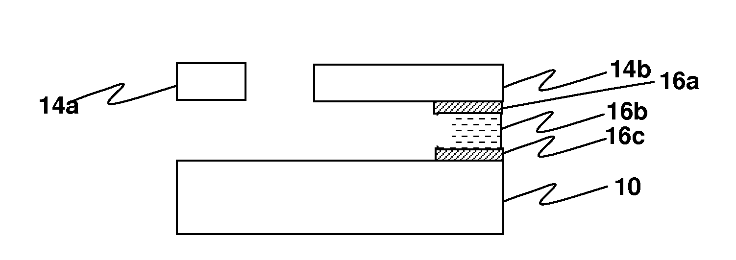
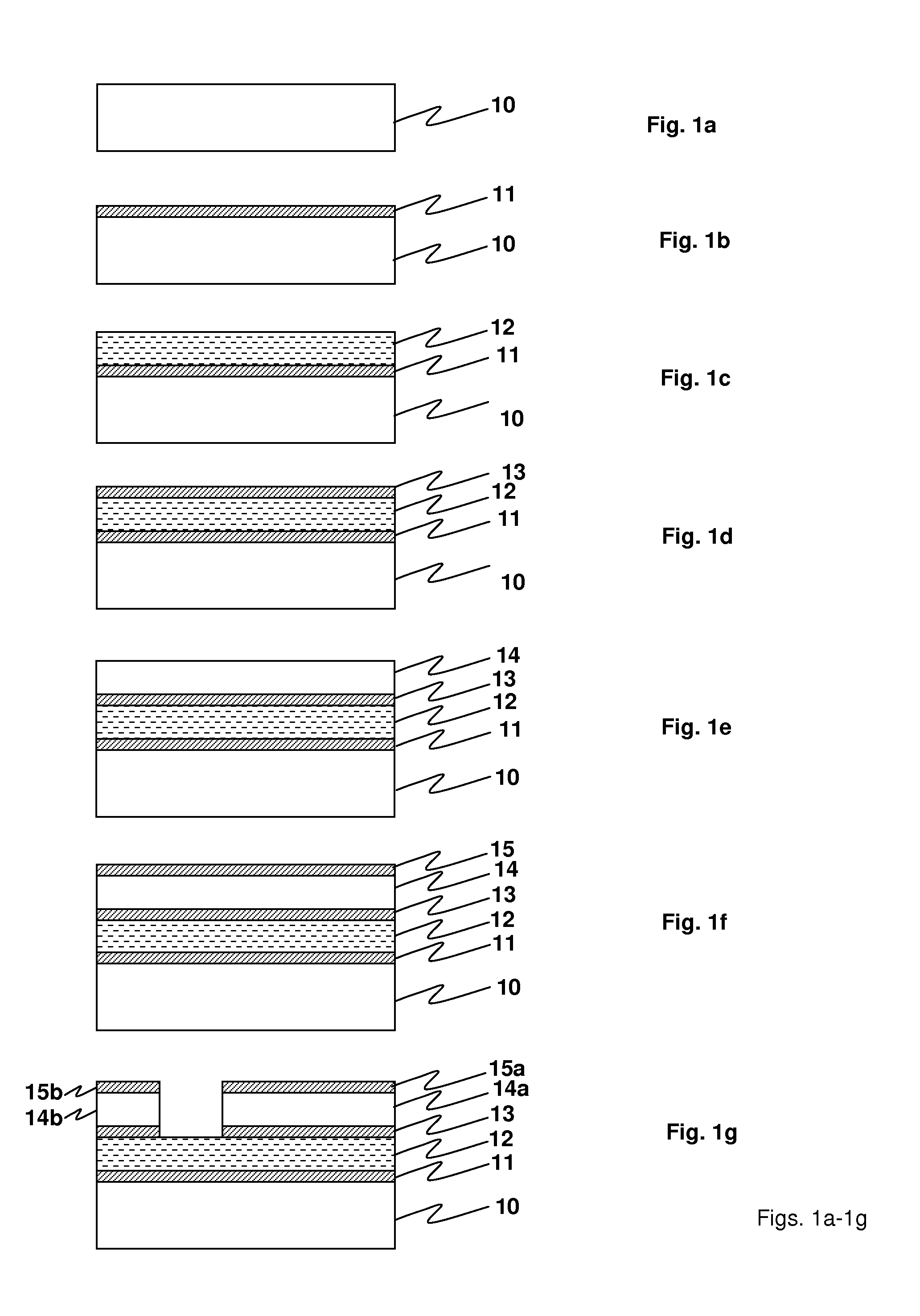
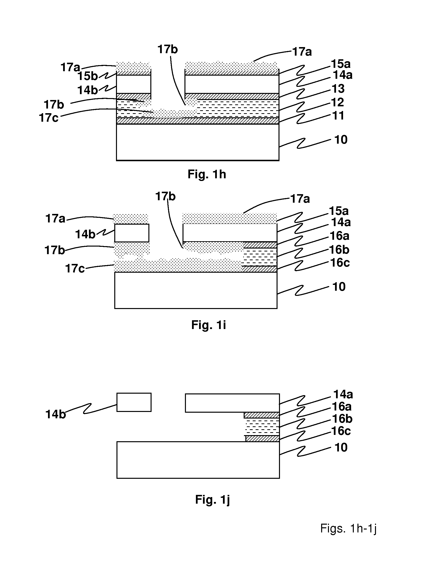
[0019]Referring first to FIGS. 1a-1j, an embodiment of an process according to the invention is illustrated wherein an NEMS stack is built and ultimately released in a series of steps. The starting substrate 10 is illustrated in FIG. 1a. One or more silicon nitride layers are deposited, depending on the embodiment. FIG. 1b illustrates a first silicon nitride layer 11, followed by deposit of a sacrificial oxide layer 12 (FIG. 1c), an intermediate silicon nitride layer 13 (FIG. 1d), a structure or device layer ...


PUM

PropertyMeasurementUnit
Thicknessaaaaaaaaaa
Volumeaaaaaaaaaa
Areaaaaaaaaaaa

Abstract

A method of avoiding stiction during vapor hydrofluoride (VHF) release of a microelectromechanical system (MEMS) or nanoelectromechanical system (NEMS) composed of a mechanical device and a substrate is described. A silicon nitride layer is provided between the substrate and a sacrificial oxide layer and/or between a device layer and the sacrificial oxide layer, and/or on a side of the device layer facing away from the sacrificial oxide layer, and converted to thicker ammonium hexafluorosilicate with VHF while simultaneously removing a portion of the sacrificial oxide. The ammonium hexafluorosilicate acts as a temporary support, shim, wedge, or tether which limits device movement during fabrication and is later removed by sublimation under heat and/or reduced pressure.

Description

BACKGROUND OF THE INVENTION[0001]This invention relates to the field of manufacturing electro-mechanical systems which includes nano-electro-mechanical systems (NEMS) and micro-electro mechanical systems (MEMS). More particularly the invention relates methods of making MEMS and NEMS using vapor hydrofluoric etching.[0002]NEMS are modern mechanical systems in which one of more of the mechanical elements are smaller than one micron in all directions. NEMS and the older technology MEMS are well known devices which consist of long thin beams that support large plates, all patterned on top of a sacrificial layer and anchored to the underlying substrate at one or more points. After the device is completed, the sacrificial layer is etched away and the plate and beams are free to move except at the anchor points.[0003]Many patents and other publications disclose various methods of making NEMS and MEMS. For example, Mastrangelo U.S. Pat. 5,258,097 disclosed a method of fabricating microstruc...

Claims


Application Information

Patent Timeline
IPC IPC(8): B81C1/00
CPCB81C1/00523B81C1/00936B81B7/02B81C1/00C23C16/40C23C16/44
Inventor VESTYCK, DANIEL J.
Owner SPTS TECH LTD
Why Eureka
Try Eureka