Method for reducing proximity effects in electron beam lithography

Inactive Publication Date: 2005-12-01
GLOBALFOUNDRIES INC
View PDF8 Cites 10 Cited by
  • Summary
  • Abstract
  • Description
  • Claims
  • Application Information

AI Technical Summary

Benefits of technology

[0010] In preferred embodiments of the invention, electron-scattering induced proximity effects are reduced by applying an electric field in or near the region where the detrimental electron backscattering occurs. Based on intuition alone, one might assume that extremely high electric fields would be required, since the electrons in the e-beam can be very ener

Problems solved by technology

Since the resist is sensitive to the deposition of energy resulting from interactions with electrons as they pass through the resist, the resolution achievable with electron beam lithography is, to a first approximation, limited by the spot size of the incident e-beam.
Although this broadening effect is important for thick resists, it is relatively unimportant for thin resists at high beam energies.
Moreover, the broadening that arises from this kind of scattering is often small compared to the intrinsic resolution of the resist.
However, they are all plagued by the fact that mathematically, the correction of proximity effects is an ill-posed problem, since a complete solution requires the application of negative exposure doses t

Method used


Image

  • Method for reducing proximity effects in electron beam lithography
  • Method for reducing proximity effects in electron beam lithography
  • Method for reducing proximity effects in electron beam lithography

Examples


Embodiment Construction

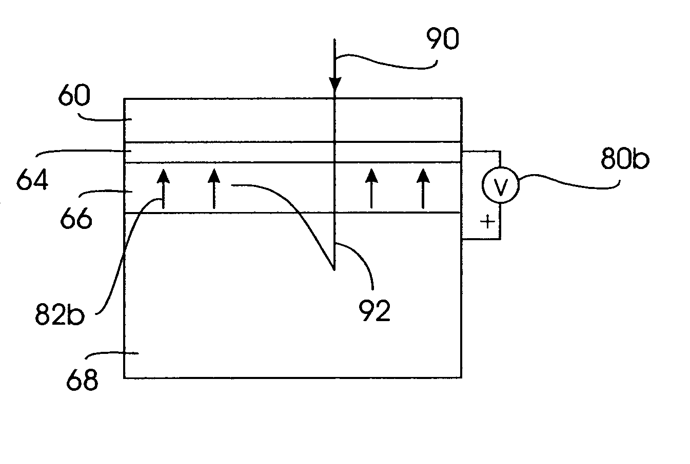
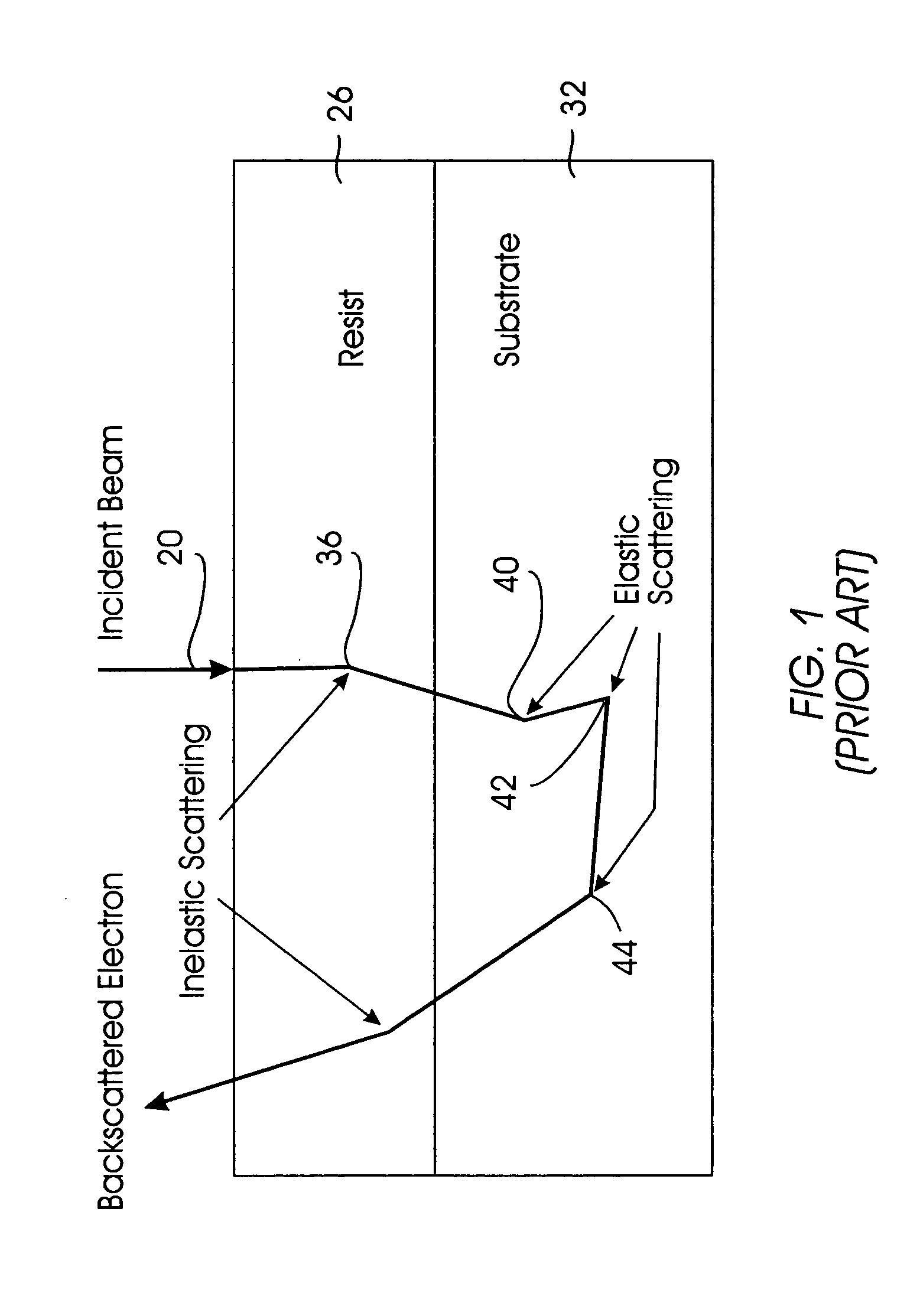
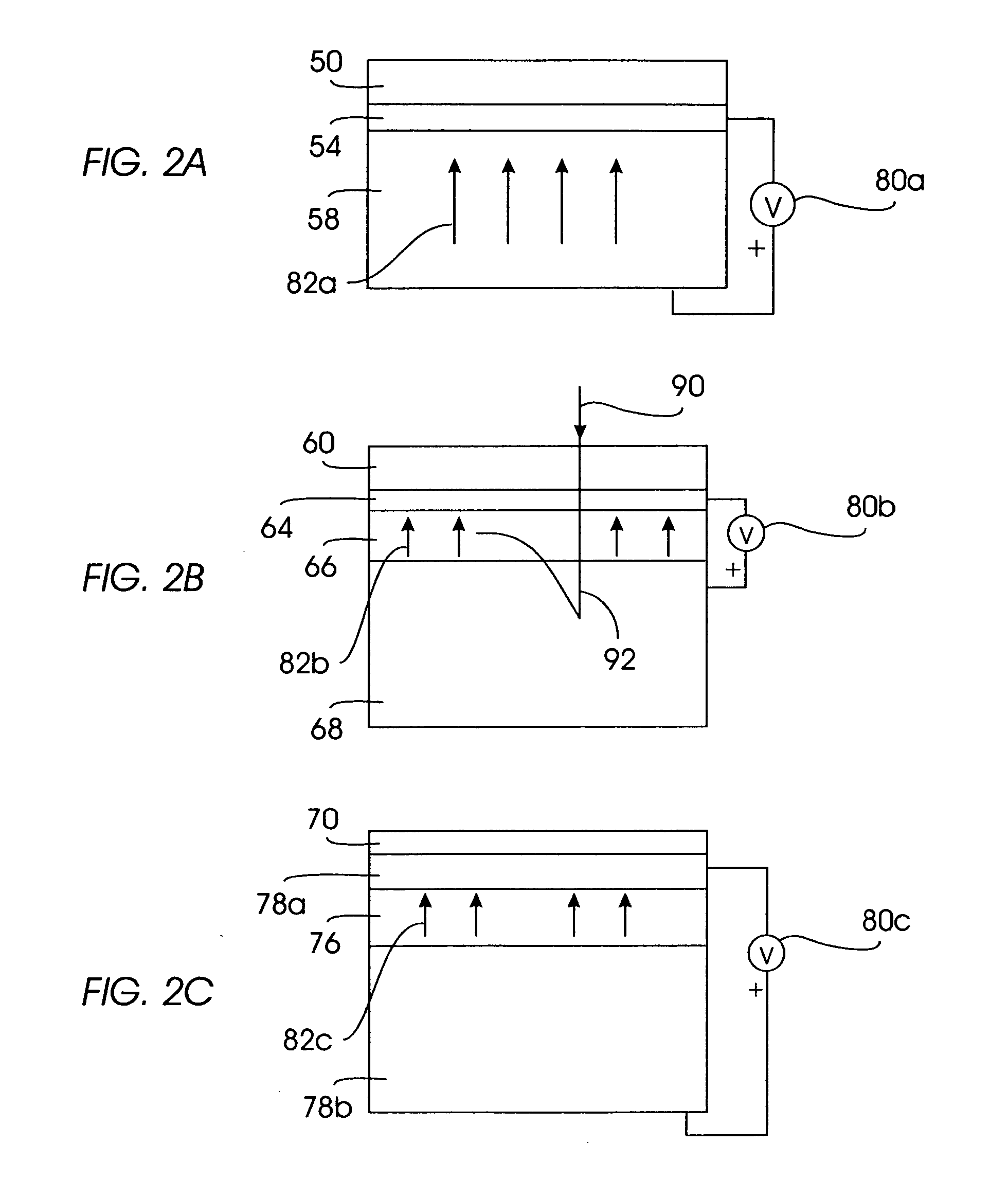
[0029] Preferred implementations of the invention disclosed herein mitigate electron scattering effects that would otherwise make it difficult to achieve high resolution, well-defined features in resist material using electron beam lithography. By modeling the behavior of electron scattering by atoms in the substrate 32 (see FIG. 1), it is possible to demonstrate how applying an electric field to the substrate can mitigate deleterious scattering effects, thereby making it possible to improve the resolution of features formed in the resist 26. The scattering of electrons by atoms can be modeled by considering that both elastic and inelastic scattering of electrons can occur, and that both kinds of scattering affect the mean free path λ of electrons propagating through a material. If the total elastic cross section and the total inelastic cross section are denoted by σe and σin, respectively, then λ-1={Σi⁢Ni⁡(σiⅇ+σiin)}(1)

in which the summation is over the different types of particl...


PUM


Abstract

An electric field is applied below a resist to reduce proximity effects associated with electron beam scattering, thereby improving the resolution of features or lines written into the resist. Although the electrons in the electron beam can be very energetic (e.g., >>10 keV), it is shown that even a small electric field can reduce the number of electrons that re-enter the resist material after being scattered in the substrate, and thus reduce the energy deposited in the resist from these electrons. One advantage of this technique is that high potentials and high fields are not required. Accordingly, the methods described can be applied to existing tooling with little modification to the electron beam system.

Description

TECHNICAL FIELD [0001] The invention relates to electron beam lithography, and more particularly to a method of reducing proximity effects associated with electron beam scattering, in order to improve the resolution and fidelity of features or lines written into a resist material. BACKGROUND [0002] Electron beam lithography (“e-beam” lithography) involves exposing a film of polymer resist, which resides on a substrate, to a beam of electrons, thereby breaking the molecular chains of the exposed polymer. In the case of a positive resist, the exposed portions of the polymer have increased solubility with respect to a solvent, so that by bringing the solvent into contact with the exposed portions, selective dissolution or etching of the resist takes place to produce empty spaces such as trenches or voids in the resist. By filling the spaces with metal and then removing the remaining (unexposed) resist, metallic structures can be fabricated that are suitable for various microelectronic ...

Claims


Application Information

Patent Timeline
IPC IPC(8): G03F7/20H01J37/302H01J37/305H01J37/317H01L21/027
CPCB82Y10/00B82Y40/00G03F1/78H01J2237/31796G03F7/2063H01J37/3174G03F7/2061
Inventor MARRIAN, CHRISTIE RODERICK KINGSLEYRETTNER, CHARLES THOMAS
Owner GLOBALFOUNDRIES INC
Why Eureka
Try Eureka