Systems and methods for reducing effects of interference in input devices

a technology of input device and interference, applied in the field of electronic devices, can solve the problems of unison noise, difficulty in identifying and/or removing some types of interference, and the particular vulnerability of implementations to various types of interference, so as to facilitate the improvement of input device performance, improve the resistance to interference, and improve the resistance to the effect of interfa

Inactive Publication Date: 2013-12-26
SYNAPTICS INC
View PDF1 Cites 10 Cited by
  • Summary
  • Abstract
  • Description
  • Claims
  • Application Information

AI Technical Summary

Benefits of technology

[0008]The embodiments of the present invention provide devices and methods that facilitate improved input device performance. Specifically, the devices and methods provide improved resistance to the effect of interference on input devices, and in particular, to the effect of unison noise on proximity sensors that use capacitive techniques to generate images of sensor values. The devices and methods provide improved resistance to the effects of interface by using multiple images of sensor values, where the multiple images of sensor values are captured at different times along two different axes. The multiple images of sensor values are combined to produce a modified image of sensor values, the modified image having reduced errors due to noise. This reduction in errors due to noise can improve the accuracy and performance of the input device.
[0009]In one embodiment, a processing system is provided for an input device having a plurality of sensor electrodes, where the processing system comprises a sensor module and a determination module. The sensor module comprises sensor circuitry configured to operate the plurality of sensor electrodes to capture first resulting signals and second resulting signals. The determination module is configured to generate a first image of sensor values from the first resulting signals, where the first image of sensor values has first errors associated with the first resulting signals being captured at different times along a first axis. The determination module is further configured to generate a second image of sensor values from the second resulting signals, where the second image of sensor values has second errors associated with the second resulting signals being captured at different times along a second axis different from the first axis. The determination module is further configured to produce a modified image of sensor values based on the first image of sensor...

Problems solved by technology

While capacitive image sensors are advantageous in a number of respects, some implementations may be particularly vulnerable to various types of interference, including various types of noise.
Although many sensors now include filtering that can effectively remove many types of interference, problems remai...

Method used


Image

  • Systems and methods for reducing effects of interference in input devices
  • Systems and methods for reducing effects of interference in input devices
  • Systems and methods for reducing effects of interference in input devices

Examples


Embodiment Construction

[0017]The following detailed description is merely exemplary in nature and is not intended to limit the invention or the application and uses of the invention. Furthermore, there is no intention to be bound by any expressed or implied theory presented in the preceding technical field, background, brief summary, or the following detailed description.

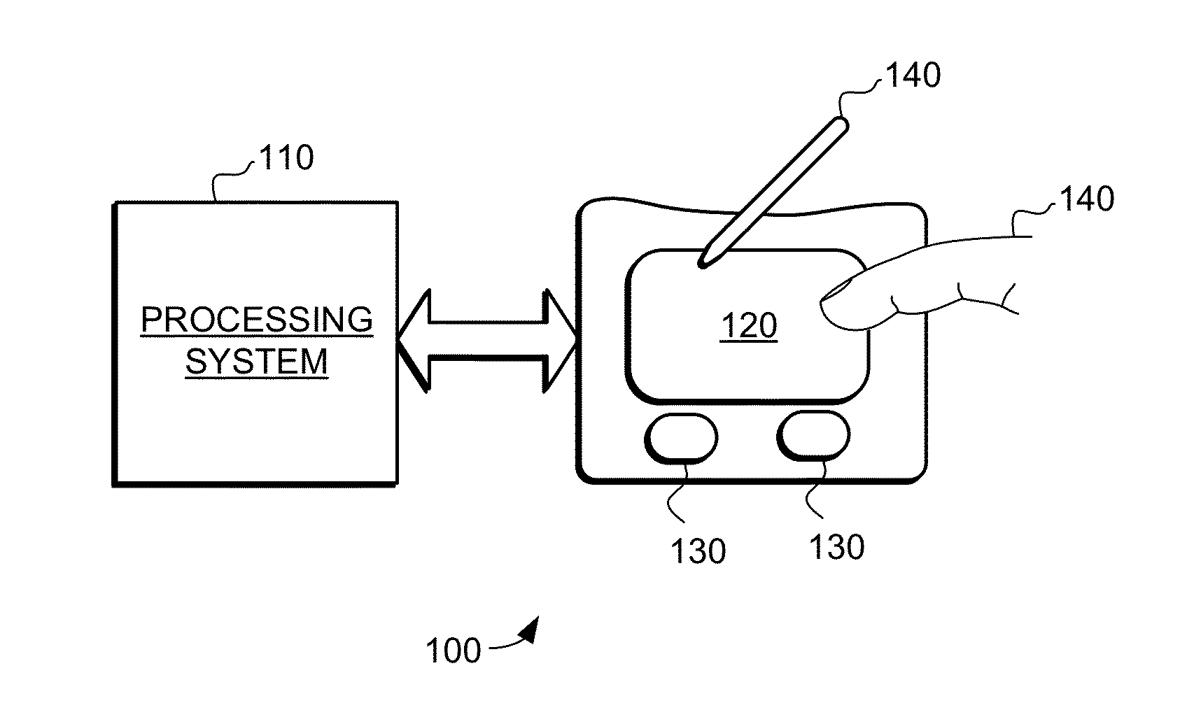
[0018]Various embodiments of the present invention provide input devices and methods that facilitate improved usability. FIG. 1 is a block diagram of an exemplary input device 100, in accordance with embodiments of the invention. The input device 100 may be configured to provide input to an electronic system (not shown). As used in this document, the term “electronic system” (or “electronic device”) broadly refers to any system capable of electronically processing information. Some non-limiting examples of electronic systems include personal computers of all sizes and shapes, such as desktop computers, laptop computers, netbook computers,...


PUM


Abstract

The embodiments described herein provide devices and methods that facilitate improved input device performance. Specifically, the devices and methods provide improved resistance to the effect of interference on input devices, and in particular, to the effect of unison noise on proximity sensors that use capacitive techniques to generate images of sensor values. The devices and methods provide improved resistance to the effects of interface by using multiple images of sensor values, where the multiple images of sensor values are captured at different times along two different axes. The multiple images of sensor values are combined to produce a modified image of sensor values, the modified image having reduced errors due to noise. This reduction in errors due to noise can improve the accuracy and performance of the input device.

Description

FIELD OF THE INVENTION[0001]This invention generally relates to electronic devices, and more specifically relates to input devices.BACKGROUND OF THE INVENTION[0002]Input devices including proximity sensor devices (also commonly called touchpads or touch sensor devices) are widely used in a variety of electronic systems. A proximity sensor device typically includes a sensing region, often demarked by a surface, in which the proximity sensor device determines the presence, location and / or motion of one or more input objects. Proximity sensor devices may be used to provide interfaces for the electronic system. For example, proximity sensor devices are often used as input devices for larger computing systems (such as opaque touchpads integrated in, or peripheral to, notebook or desktop computers, or as transparent sensor devices integrated with display screens to provide a touch screen interface).[0003]Many proximity sensor devices use capacitive techniques to sense input objects. Such ...

Claims


Application Information

Patent Timeline
IPC IPC(8): G06F19/00
CPCG06F3/0446G06F3/04184G06F3/0443
Inventor BULEA, MIHAI
Owner SYNAPTICS INC
Why Eureka
Try Eureka