Sealing resin sheet, method for producing electronic component package and electronic component package

a technology of sealing resin and electronic components, applied in the direction of record information storage, instruments, transportation and packaging, etc., can solve the problems of deteriorating reliability of electronic components, reducing adhesion with electrodes, and no longer being able to achieve precise mounting

Inactive Publication Date: 2014-01-09
NITTO DENKO CORP
View PDF2 Cites 29 Cited by
  • Summary
  • Abstract
  • Description
  • Claims
  • Application Information

AI Technical Summary

Benefits of technology

[0007]An object of the present invention is to provide a sealing resin sheet, wherein a clean, smooth and flat ground surface is obtained by grinding after resin sealing, a method for producing an electronic component package using the sealing resin sheet, and an electronic component package obtained by the production method.

Problems solved by technology

If the mean surface roughness Ra is more than 1 μm, an unevenness of the ground surface becomes so large that a height difference occurs in an electrode formed on the surface of an electronic component, an electrode that is formed in a subsequent step, or the like, leading to a reduction in adhesion with electrodes or the like of a substrate, so that precise mounting can no longer be achieved, and cracking easily occurs during heat treatment of a ground product, or the like, so that the reliability of an electronic component package is deteriorated.

Method used


Image

  • Sealing resin sheet, method for producing electronic component package and electronic component package
  • Sealing resin sheet, method for producing electronic component package and electronic component package
  • Sealing resin sheet, method for producing electronic component package and electronic component package

Examples


first embodiment

Sealing Resin Sheet

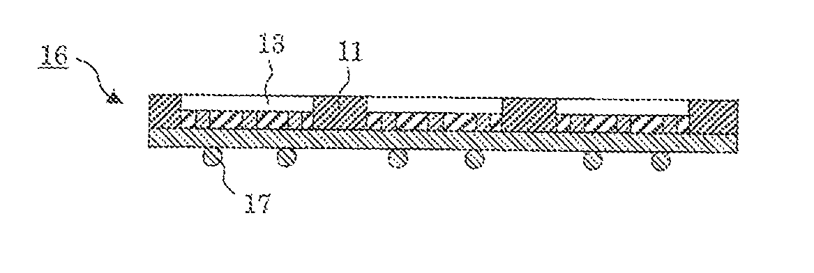
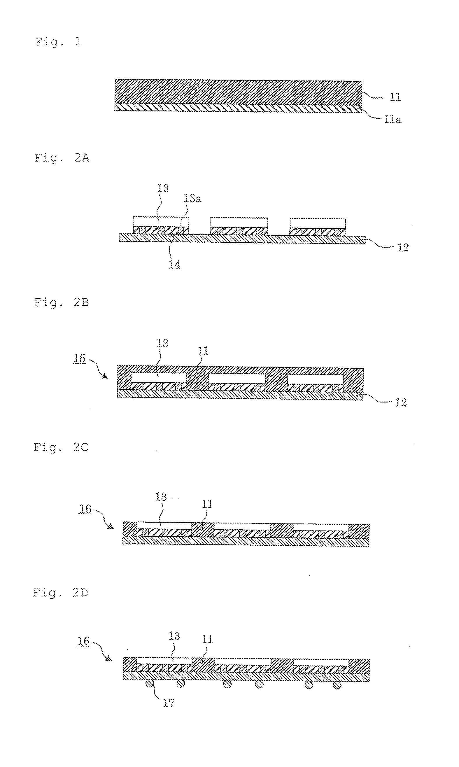
[0041]A sealing resin sheet according to this embodiment will be described with reference to FIG. 1. FIG. 1 is a sectional view schematically showing a sealing resin sheet according to one embodiment of the present invention. A sealing resin sheet 11 is typically provided in a state of being laminated on a support 11a such as a polyethylene terephthalate (PET) film. The support 11a may be subjected to a mold release treatment for easily peeling off the sealing resin sheet 11.

[0042]In the sealing resin sheet 11, a ground surface has a mean surface roughness Ra of 1 μm or less when grinding is performed under conditions including a grind bite peripheral velocity of 1000 m / minute, a feed pitch of 100 μm and a cut depth of 10 μm after a heat curing treatment is performed at 180° C. for 1 hour; and a Shore D hardness at 100° C. after the heat curing treatment is 70 or more. The ground surface preferably has a mean surface roughness Ra of 0.5 μm or less, more preferably...

second embodiment

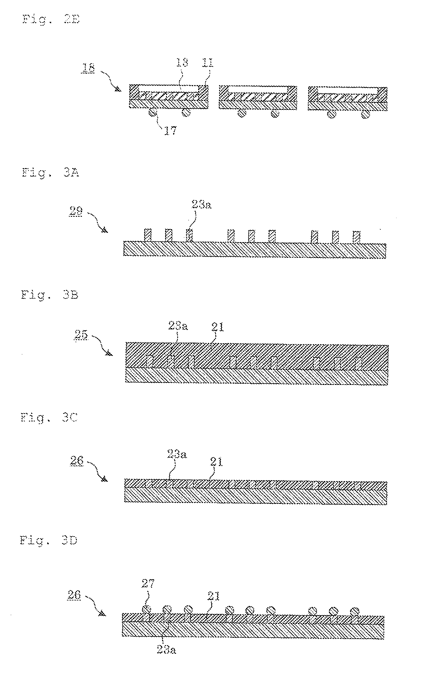
[0100]Next, a second embodiment of the present invention will be described. In the first embodiment, a production method suitable for production of a flip chip-type mounting substrate has been described, but in the second embodiment, a production method suitable for production of an electronic component package referred to as a Fan-in-type wafer level package (WLP) is described. FIGS. 3A to 3E are sectional views each schematically showing one step of a method for producing an electronic component package according to the second embodiment of the present invention.

(Semiconductor Wafer Providing Step)

[0101]A plurality of projecting electrodes 23a may be formed on one surface of a semiconductor wafer 29 (see FIG. 3A), or projecting electrodes may be formed on both surfaces of the semiconductor wafer 29 (not shown). The material of the projecting electrode such as a bump or a conductive material is not particularly limited, and examples thereof include solders (alloys) such as a tin-le...

third embodiment

[0109]A third embodiment of the present invention will be described below. FIGS. 4A to 4G are sectional views each schematically showing one step of a method for producing an electronic component package according to still another embodiment of the present invention. In the first embodiment, semiconductor chips mounted on a printed wiring substrate are resin-sealed with a sealing resin sheet, but in the third embodiment, semiconductor chips are resin-sealed while the semiconductor chips are temporarily fixed on a temporary fixing material rather than an adherend such as a substrate. The third embodiment is suitable for production of an electronic component package referred to as a Fan-out-type wafer level package (WLP).

[Temporary Fixing Material Providing Step]

[0110]In a temporary fixing material providing step, a temporary fixing material 3 in which a thermally expandable pressure-sensitive adhesive layer 3a is laminated on a support 3b is provided (see FIG. 4A). A radiation-curabl...


PUM


Abstract

Provided are a sealing resin sheet, wherein a clean, smooth and flat ground surface is obtained by grinding after resin sealing, a method for producing an electronic component package using the same, and an electronic component package obtained by the production method. The present invention provides a sealing resin sheet, wherein a ground surface has a mean surface roughness Ra of 1 μm or less when grinding is performed under conditions of a grind bite peripheral velocity of 1000 m/minute, a feed pitch of 100 μm and a cut depth of 10 μm after a heat curing treatment is performed at 180° C. for 1 hour; and a Shore D hardness at 100° C. after the heat curing treatment is 70 or more.

Description

BACKGROUND OF THE INVENTION[0001]1. Field of the Invention[0002]The present invention relates to a sealing resin sheet, a method for producing an electronic component package and an electronic component package.[0003]2. Description of the Related Art[0004]In recent years, downsizing, weight reduction and function enhancement of electronic instruments have been increasingly required, and accordingly downsizing, thickness reduction and high density mounting have been desired for packages that form electronic instruments.[0005]For preparation of an electronic component package, typically a procedure is employed in which electronic components that are fixed to a substrate, a temporary fixing material or the like are sealed with a sealing resin, and the sealed product is diced as necessary so that a package is formed per each electronic component. For meeting the above-described requirement, in the course of this process, a technique of reducing the thickness by grinding (back-grinding) ...

Claims


Application Information

Patent Timeline
Patent Type & Authority Applications(United States)
IPC IPC(8): H01L21/56H01L23/29
CPCH01L21/56H01L23/29H01L23/3128H01L24/19H01L24/96H01L2924/18162H01L24/97H01L2224/12105H01L2224/16225H01L2224/32225H01L2224/73204H01L2224/94H01L2224/97H01L2924/15311H01L2924/18161H01L2924/181H01L2924/12042H01L2924/3511Y10T428/24355H01L2224/83H01L2224/81H01L2224/11H01L2924/00H01L23/28
Inventor TOYODA, EIJISHIMIZU, YUSAKU
Owner NITTO DENKO CORP
Why Eureka
Try Eureka