Coil component

a technology of coils and components, applied in the direction of coil manufacturing, transformer/inductance details, inductances, etc., can solve the problems of affecting the quality of coils, the failure of electrical connections, and the inability to form desired spiral patterns, so as to reduce material costs, prevent thickening of outermost turns, and increase the mounting strength of solder connections

Active Publication Date: 2014-01-09
TDK CORPARATION
View PDF17 Cites 126 Cited by
  • Summary
  • Abstract
  • Description
  • Claims
  • Application Information

AI Technical Summary

Benefits of technology

[0032]According to the present invention, the provision of the first and second dummy terminal electrodes along with the first and second spiral conductors can prevent thickening of the outermost turns of the first and second spiral conductors, respectively. The outer side surface of the first terminal electrode and the outer side surface of the first dummy terminal electrode are exposed at the side surfaces of the coil component. At the time of surface mounting, solder fillets can thus be formed to increase the mounting strength of the solder connection. The exposed surfaces of the substrate function as stopper surfaces for suppressing the formation of solder fillets. This can prevent the solder fillets from being formed up to the exposed surface of the second dummy terminal electrode exposed along with the first terminal electrode and the exposed surface of the second terminal electrode exposed along with the first dummy terminal electrode. The solder fillets can thus be formed with a minimum amount of solder, which can reduce the material cost. Such a configuration can also prevent solder melted or re-melted in a reflow step from creeping up the side electrodes to reach a shield cover covering an upper part of the coil component, if any, and cause an electrical connection failure.
[0033]In the present invention, the substrate may include first and second side surfaces that are parallel to each other, and third and fourth side surfaces that are orthogonal to the first and second side surfaces. The first side surface of the substrate may form the same plane as the outer side surface of the first terminal electrode and the outer side surface of the second dummy terminal electrode. The second side surface of the substrate may form the same plane as the outer side surface of the second terminal electrode and the outer side surface of the first dummy terminal electrode. According to such a configuration, a solder fillet can be formed on each of the plurality of side electrodes at the time of surface mounting, whereby the mounting strength of the solder connection can be improved. The solder fillets can also be formed with a minimum amount of solder, which can reduce the material cost.
[0034]The

Problems solved by technology

However, HAP can sometimes cause an abnormal lateral growth of the plating layer at a portion corresponding to the outermost turn of the planar spiral conductor.
The outermost turn therefore becomes excessively large in line width, causing the problem that a desired spi

Method used


Image

  • Coil component
  • Coil component
  • Coil component

Examples


first embodiment

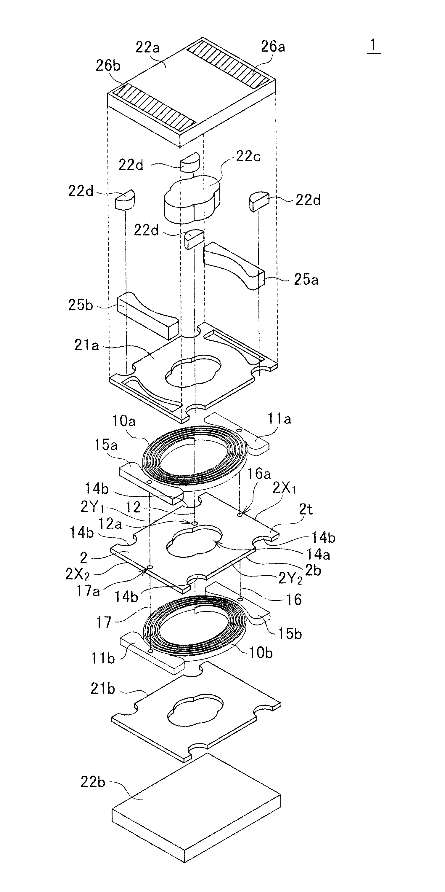
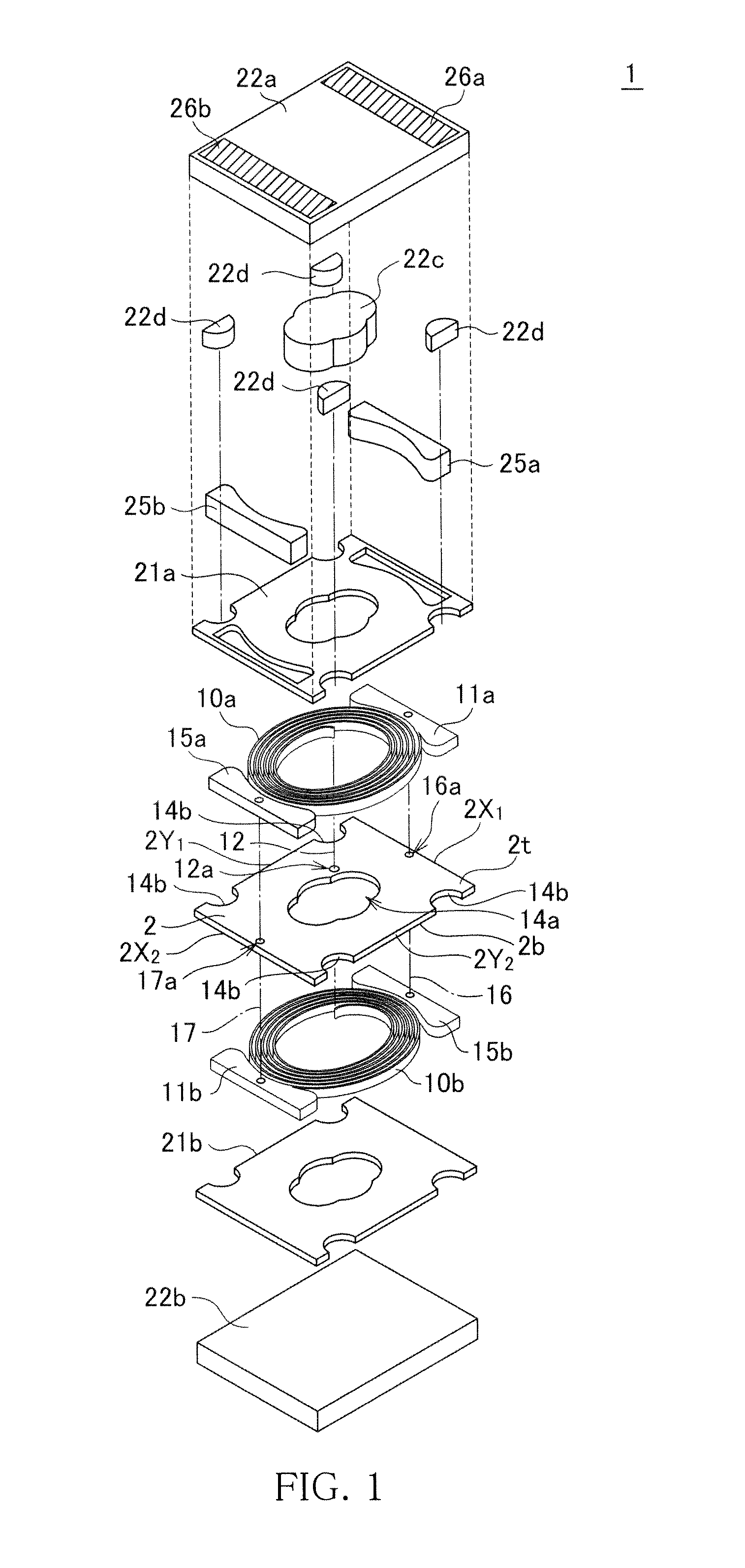
[0068]FIG. 1 is an exploded perspective view of a coil component 1 according to the present invention. As shown in the diagram, the coil component 1 includes a substrate 2 of generally rectangular shape. The “generally rectangular shape” shall include not only a perfect rectangle but also a rectangular shape partly notched in corners. As employed herein, the term “corner portions” of a rectangular shape that is partly notched in corners refers to the corner portions of a perfect rectangle that would be obtained without the notches.

[0069]The substrate 2 is preferably made of a typical printed-circuit board which is obtained by impregnating a glass cloth with epoxy resin. For example, a BT resin substrate, an FR4 substrate, or an FR5 substrate may be used.

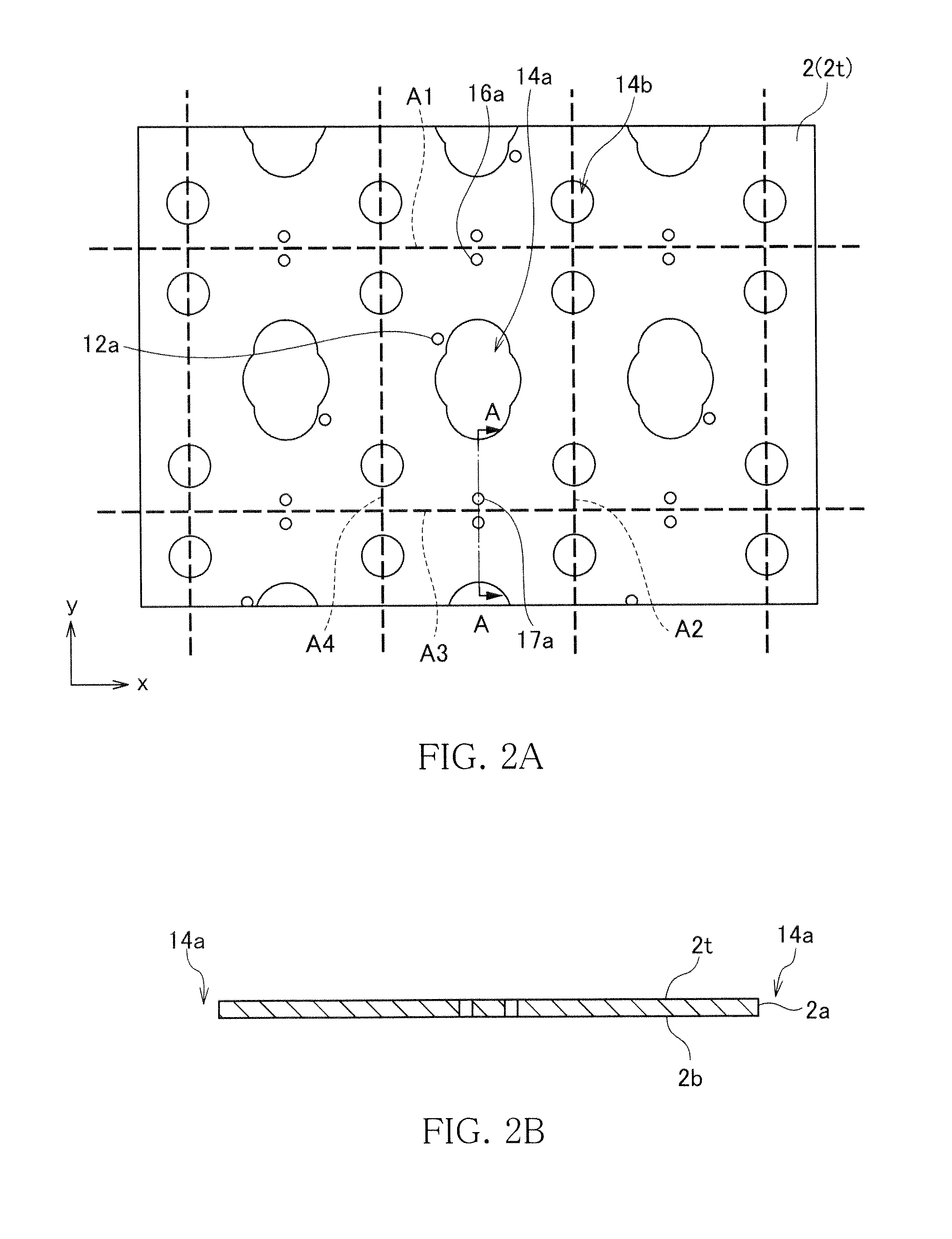
[0070]A planar spiral conductor 10a (first planar spiral conductor) is formed on a center portion of a top surface 2t of the substrate 2. A planar spiral conductor 10b (second planar spiral conductor) is similarly formed on a center ...

second embodiment

[0118]FIG. 12 is a schematic perspective view showing an appearance and shape of a coil component 3 according to the present invention.

[0119]As shown in FIG. 12, the coil component 3 according to the present embodiment is a chip component of surface mounting type. The coil component 3 includes a thin-film coil layer 5 including planar coil conductors, and first and second metal magnetic powder-containing resin layers 37 and 38 stacked on top and bottom of the thin-film coil layer 5. The coil component 3 has a rectangular solid shape in outline, and has a top surface 3a, a bottom surface 3b, and four side surfaces 3c to 3f.

[0120]A pair of external electrodes 48 and 49 are formed on the top surface 3a of the coil component 3 (the main surface of the first metal magnetic powder-containing resin layer 37). A pair of side electrodes 50 and 51 are arranged on two opposed side surfaces 3c and 3d of the coil component 3, respectively. The external electrode 48 and the side electrode 50 are...

third embodiment

[0170]FIG. 22 is a schematic exploded perspective view showing the configuration of a coil component 4 according to the present invention.

[0171]As shown in FIG. 22, the coil component 4 according to the present embodiment is characterized by that the through-hole magnetic bodies 25 arranged in the corner portions of the substrate 30 are omitted. The substrate 30 has no through-hole 30h. The side surfaces 30c and 30d of the substrate 30 have the same width as the maximum width of the substrate. Being tailored to the shape of the substrate 30, the first and second terminal electrodes 33 and 34 and the first and second dummy terminal electrodes 35 and 36 also have the same width as that of the side surfaces 30c and 30d. According to the present embodiment, like the coil component 3 according to the second embodiment, the side surfaces 30c and 30d of the substrate 30 sandwiched between the terminal electrodes 33 and 34 and the dummy terminal electrodes 35 and 36 are exposed along with t...


PUM


Abstract

A coil component 1 includes a substrate 2, a planar spiral conductor 10a formed on a top surface 2t of the substrate 2, a lead conductor 11a connected to an outer peripheral end of the planar spiral conductor 10a, a dummy lead conductor 15a formed on the top surface of the substrate 2 and between an outermost turn of the planar spiral conductor 10a and an end 2X2 of the substrate 2 and free from an electrical connection with another conductor within the same plane, external electrodes 26a and 26b arranged in parallel with the top surface of the substrate 2, and a bump electrode 25a formed on a surface of the lead conductor 11a and connects the lead conductor 11a with the external electrode 26a. The external terminals 26a and 26b have a larger area than the bump electrodes 15a and 15b for securing a bonding strength.

Description

BACKGROUND OF THE INVENTION[0001]1. Field of the Invention[0002]The present invention relates to a coil component. In particular, the present invention relates to a coil component including a planar spiral conductor formed on a printed-circuit board by electrolytic plating and a method for manufacturing the same.[0003]2. Description of Related Art[0004]In the field of consumer and industrial electronic devices, surface-mounting type coil components have been used more and more as power supply inductors. The reason is that surface-mounting type coil components are small and thin, provide excellent electrical insulation, and can be manufactured at low cost.[0005]Among specific structures of a surface-mounting type coil component is a planar coil structure using printed-circuit board technology (for example, see Japanese Patent No. 4873049). The structure will be briefly described in terms of manufacturing steps. Initially, a seed layer (base film) having a planar spiral shape is forme...

Claims


Application Information

Patent Timeline
IPC IPC(8): H01F27/28
CPCH01F27/2804H01F17/0033H01F27/022H01F27/255H01F27/292H01F2017/0073H01F17/00H01F41/04H01F27/29H01F2027/2809
Inventor OHKUBO, HITOSHIITO, TOMOKAZUITOH, HIDETOMAEDA, YOSHIHIROOHTA, MANABUKANAME, YUUYAKAWAHARA, TAKAHIRONAKAGAWA, TAKASHI
Owner TDK CORPARATION
Why Eureka
Try Eureka