

Hybrid computing module
- Summary
- Abstract
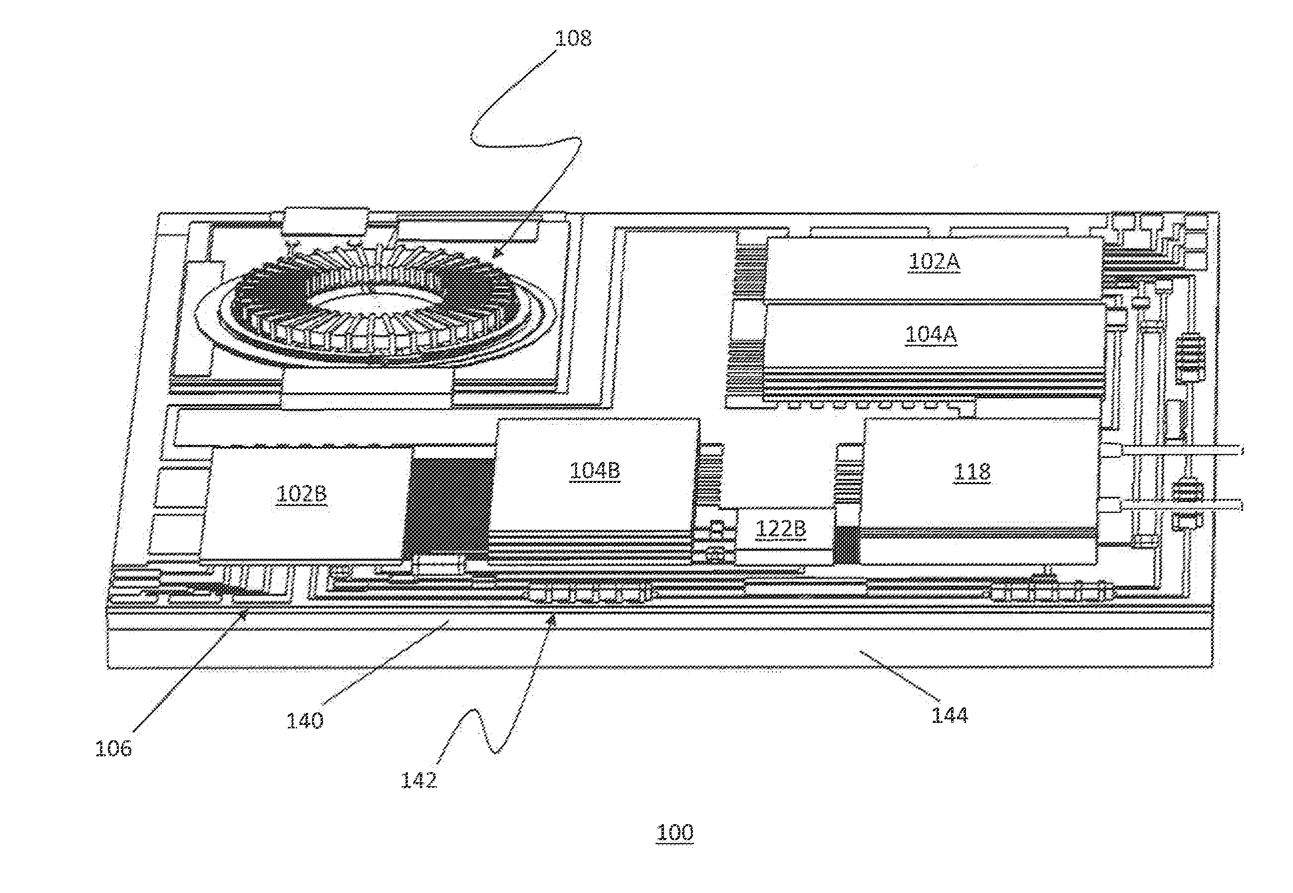
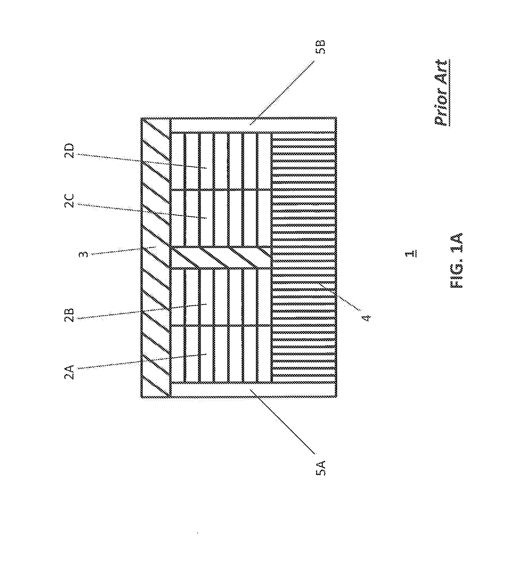
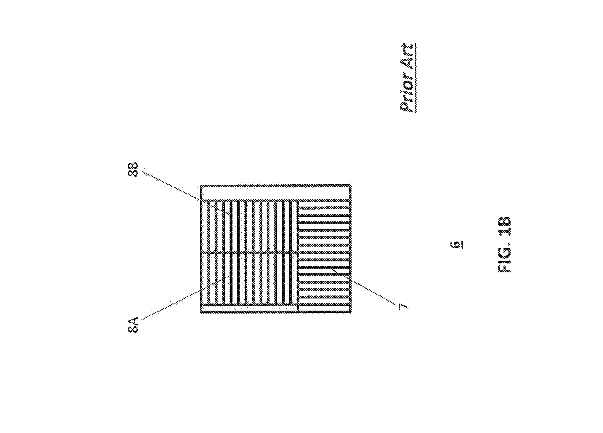
- Description
- Claims
- Application Information
AI Technical Summary
Benefits of technology
Problems solved by technology
Method used
Image

Examples
Embodiment Construction
[0086]The present invention is illustratively described above in reference to the disclosed embodiments. Various modifications and changes may be made to the disclosed embodiments by persons skilled in the art without departing from the scope of the present invention as defined in the appended claims.
[0087]This application incorporates by reference all matter contained in de Rochemont U.S. Pat. No. 7,405,698 entitled “CERAMIC ANTENNA MODULE AND METHODS OF MANUFACTURE THEREOF” (the '698 application), de Rochemont U.S. Ser. No. 11 / 479,159, filed Jun. 30, 2006, entitled “ELECTRICAL COMPONENT AND METHOD OF MANUFACTURE” (the '159 application), U.S. Ser. No. 11 / 620,042 (the '042 application), filed Jan. 6, 2007 entitled “POWER MANAGEMENT MODULES”, de Rochemont and Kovacs, “LIQUID CHEMICAL DEPOSITION PROCESS APPARATUS AND EMBODIMENTS”, U.S. Ser. No. 12 / 843,112, ('112), de Rochemont, “MONOLITHIC DC / DC POWER MANAGEMENT MODULE WITH SURFACE FET”, U.S. Ser. No. 13 / 152,222 ('222), de Rochemont, ...
PUM
 Abstract
Description
Claims
Application Information