Perpendicular sttmram device with balanced reference layer

a reference layer and parallel sttmram technology, applied in the field of magnetic memory elements, can solve the problems of preventing the advancement of the use of mtjs, the current and threshold voltage requirements are currently too high to allow practical applications of spin torque transfer based mtj, and the effect of lowering the effective h

Active Publication Date: 2014-01-16
AVALANCHE TECH
View PDF9 Cites 62 Cited by
  • Summary
  • Abstract
  • Description
  • Claims
  • Application Information

AI Technical Summary

Benefits of technology

[0027]FIG. 9 shows a graph of the performance of the element 30 when various ...

Problems solved by technology

However, a problem that is consistently experienced and that prevents advancement of the use of MTJs is the threshold voltage or current used to switch the free layer magnetization during a write.
Such current and threshold voltage requirements are currently too high to allow p...

Method used


Image

  • Perpendicular sttmram device with balanced reference layer
  • Perpendicular sttmram device with balanced reference layer
  • Perpendicular sttmram device with balanced reference layer

Examples


example 1

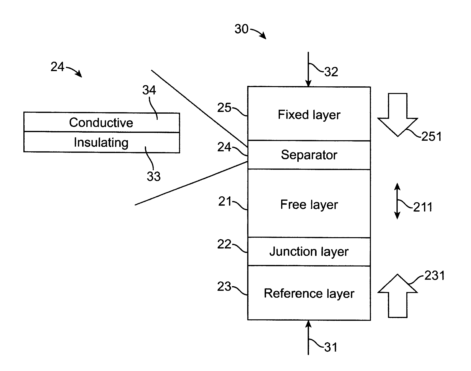
[0101]the second reference sublayer 504 formed of repeated base pairs of Co / Pt, or Co / Pd, or Co / Ni super-lattice structure with the FCC lattice;[0102]the coupling layer 506 formed of Ta with a thickness range of about 0.3 nm to about 0.8 nm;[0103]the first reference sublayer 503 formed of a CoFeB alloy and having an interface layer with the BCC lattice structure next to the junction layer 502;[0104]the junction layer 502 formed of MgO with a cubic lattice structure;[0105]the magnetic free layer 501 formed of a CoFeB alloy and having an interface layer with the BCC lattice structure next to the junction layer 502;[0106]the tuning layer 507 formed of Ta with a thickness range of about 2 nm or thicker; and[0107]the magnetic pinned layer 505 formed of repeated base pairs of Co / Pt, or Co / Pd, or Co / Ni super-lattice structure with the FCC lattice.

example 2

[0108]the second reference sublayer 504 formed of repeated base pairs of Co / Pt, or Co / Pd, or Co / Ni super-lattice structure with the FCC lattice;[0109]the coupling layer 506 formed of Ta with a thickness of about 2 nm or thicker;[0110]the first reference sublayer 503 formed of a CoFeB alloy and having an interface layer with the BCC lattice structure next to the junction layer 502;[0111]the junction layer 502 formed of MgO with a cubic lattice structure;[0112]the magnetic free layer 501 formed of a CoFeB alloy and having an interface layer with the BCC lattice structure next to the junction layer 502;[0113]the tuning layer 507 formed of Ta with a thickness range of about 2 nm or thicker; and[0114]the magnetic pinned layer 505 formed of repeated base pairs of Co / Pt, or Co / Pd, or Co / Ni super-lattice structure with the FCC lattice.

example 3

[0115]the second reference sublayer 504 formed of repeated base pairs of Co / Pt, or Co / Pd, or Co / Ni super-lattice structure with the FCC lattice;[0116]the coupling layer 506 formed of Ta with a thickness range of about 0.3 nm to about 0.8 nm;[0117]the first reference sublayer 503 formed of a CoFeB alloy and having an interface layer with the BCC lattice structure next to the junction layer 502;[0118]the junction layer 502 formed of MgO with a cubic lattice structure;[0119]the magnetic free layer 501 formed of a CoFeB alloy and having an interface layer with the BCC lattice structure next to the junction layer 502;[0120]the tuning layer 507 having a MgO / CoFeB / Ta structure, where the MgO layer with a thickness range of about 0.5 nm to about 1.1 nm is formed adjacent to the magnetic free layer 501; the CoFeB layer has a thickness range of about 0.2 nm to 0.6 nm; and the Ta layer with a thickness range of about 2 nm to about 3 nm is formed adjacent to the magnetic pinned layer 505; and[0...


PUM


Abstract

A spin toque transfer magnetic random access memory (STTMRAM) element comprises a reference layer, which can be a single layer structure or a synthetic multi-layer structure, formed on a substrate, with a fixed perpendicular magnetic component. A junction layer is formed on top of the reference layer and a free layer is formed on top of the junction layer with a perpendicular magnetic orientation, at substantially its center of the free layer and switchable. A tuning layer is formed on top of the free layer and a fixed layer is formed on top of the tuning layer, the fixed layer has a fixed perpendicular magnetic component opposite to that of the reference layer. The magnetic orientation of the free layer switches relative to that of the fixed layer. The perpendicular magnetic components of the fixed layer and the reference layer substantially cancel each other and the free layer has an in-plane edge magnetization field.

Description

CROSS REFERENCE TO RELATED APPLICATIONS[0001]This application is a continuation-in-part of the commonly assigned application bearing Ser. No. 13 / 029,054 filed on Feb. 16, 2011 by Zhou et al. and entitled “Magnetic Random Access Memory With Field Compensating Layer and Multi-Level Cell,” and a continuation-in-part of the commonly assigned application bearing Ser. No. 13 / 277,187 filed on Oct. 19, 2011 by Yiming Huai et al., and entitled “Memory System Having Thermally Stable Perpendicular Magneto Tunnel Junction (MTJ) and A Method of Manufacturing Same,” which claims priority to U.S. Provisional Application No. 61 / 483,314 and is a continuation-in-part of the commonly assigned application bearing Ser. No. 12 / 965,733 filed on Dec. 10, 2010 by Zhou et al., and entitled “Enhanced Magnetic Stiffness and Method of Making Same.” The present application is related to the commonly assigned copending application bearing Ser. No. 13 / 737,897 filed on Jan. 9, 2013, the commonly assigned copending ...

Claims


Application Information

Patent Timeline
IPC IPC(8): H01L29/82
CPCH01L29/82B82Y40/00G11C11/161H01F10/3286H01F10/329H01F10/3295H01F41/302H01L29/66984H10N50/10
Inventor GAN, HUADONGZHOU, YUCHENHUAI, YIMING
Owner AVALANCHE TECH
Why Eureka
Try Eureka