

Method for Driving Display Device and Display Device
a display device and display device technology, applied in the direction of electric digital data processing, instruments, computing, etc., can solve the problems of increasing power consumption and video signal potential change, and achieve the effect of reducing power consumption, reducing the frequency of inversion driving when video signals are written into each pixel, and reducing the amount of video signal potential change attributed to inversion driving
- Summary
- Abstract
- Description
- Claims
- Application Information
AI Technical Summary
Benefits of technology
Problems solved by technology
Method used
Image

Examples
embodiment 1
[0041]In this embodiment, one mode of a liquid crystal display device and one mode of a method for driving the liquid crystal display device are described with reference to FIGS. 1A and 1B, FIG. 2, FIGS. 3A to 3C, FIG. 4, FIG. 5, FIG. 6, FIGS. 7A and 7B, FIGS. 8A to 8C, and FIGS. 9A and 9B.
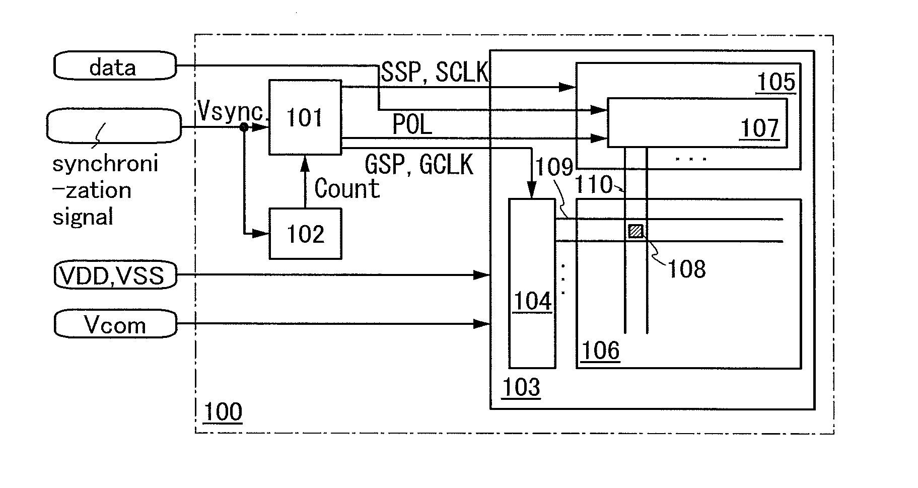
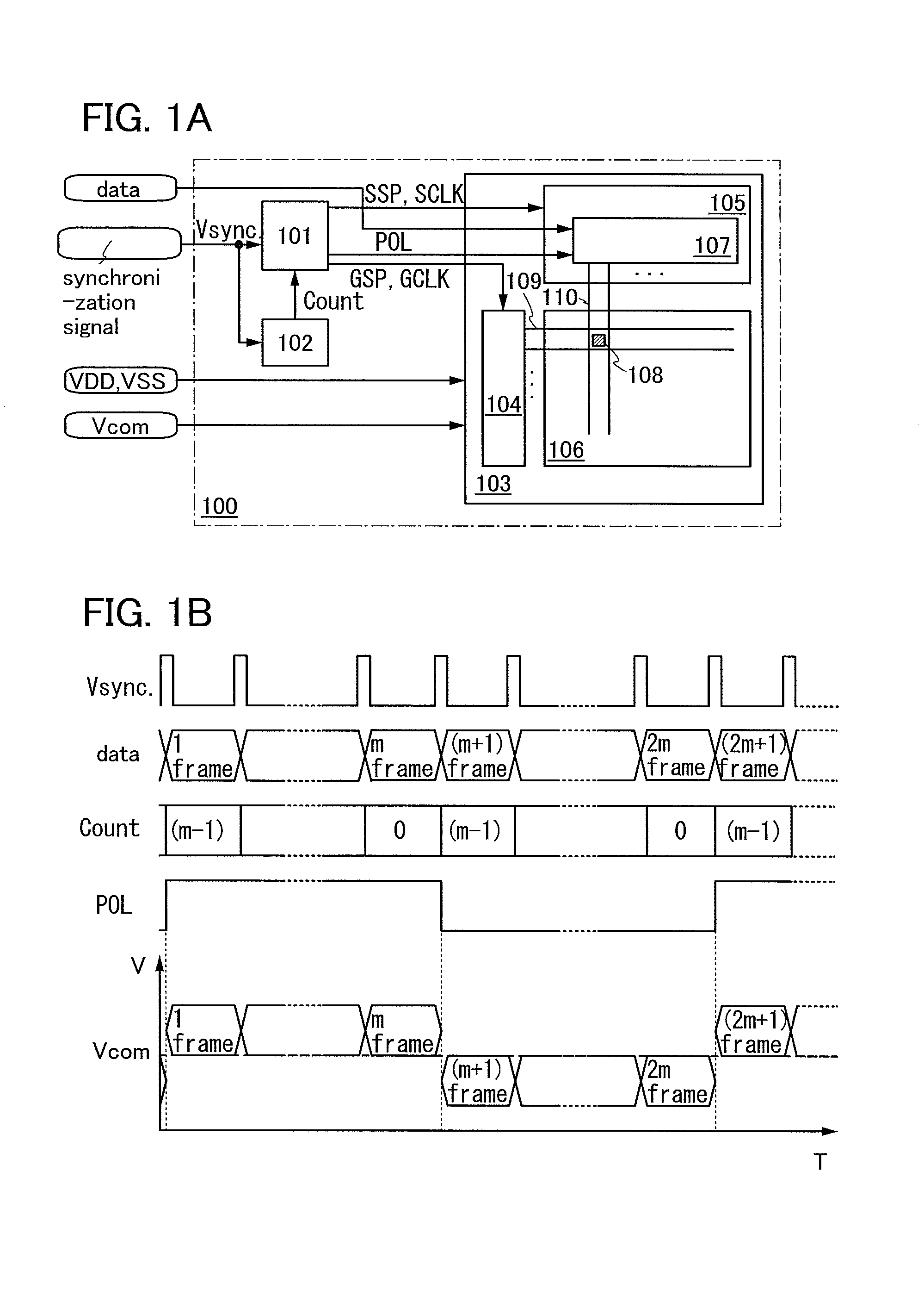
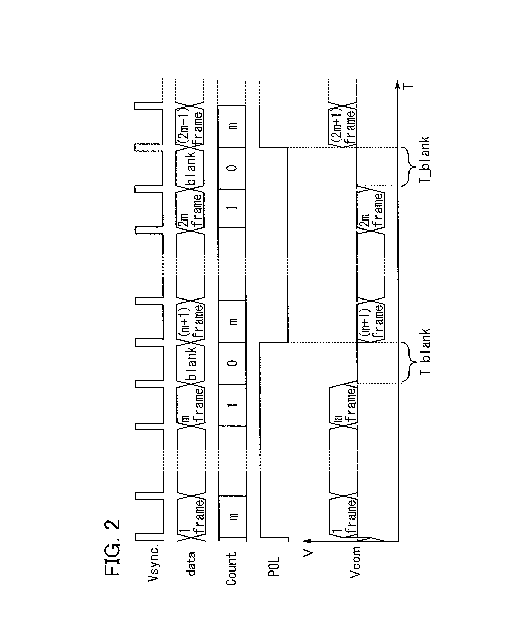
[0042]FIG. 1A is a block diagram illustrating one embodiment of a liquid crystal display device. A liquid crystal display device 100 in FIG. 1A includes a display control signal generation circuit 101, a counter circuit 102, and a display panel 103.
[0043]The display panel 103 includes a gate line driver circuit 104, a source line driver circuit 105, and a pixel portion 106. The source line driver circuit 105 includes a digital / analog conversion circuit 107. The pixel portion 106 includes a plurality of pixels 108. In the pixel 108, a scan signal supplied to a gate line 109 controls writing of a video signal supplied to a source line 110.
[0044]Power supply voltages based on a high power supply pote...
embodiment 2
[0104]In this embodiment, an external view, a cross section, and the like of the display device are illustrated and a structure thereof is described. In this embodiment, an example in which a liquid crystal element is used as the display element is given.
[0105]Note that the term “liquid crystal display device” includes any of the following modules in its category: a module provided with a connector, for example, a flexible printed circuit (FPC), a tape automated bonding (TAB) tape, or a tape carrier package (TCP); a module provided with a printed wiring board at the end of a TCP; and a module where an integrated circuit (IC) is directly mounted on a display element by a chip on glass (COG) method.
[0106]An external view and a cross section of a liquid crystal display device are described with reference to FIGS. 10A1, 10A2, and 10B. FIGS. 10A1 and 10A2 are plan views of a panel in which transistors 4010 and 4011 and a liquid crystal element 4013 are sealed between a first substrate 40...
embodiment 3
[0125]This embodiment shows the display mode of the liquid crystal element described in Embodiment 2. Although Embodiment 2 shows an example of the cross section of a twisted nematic (TN) mode liquid crystal element, the liquid crystal element can employ another display mode. Electrodes and substrates used for operating liquid crystal in various display modes will be described below with reference to schematic views.
[0126]FIG. 11 is a schematic view illustrating a cross section of a TN mode liquid crystal element.
[0127]A liquid crystal layer 5800 is sandwiched between a first substrate 5801 and a second substrate 5802 that are placed opposite to each other. A first electrode 5805 is formed on the first substrate 5801. A second electrode 5806 is formed over the second substrate 5802.
[0128]FIG. 12A is a schematic view illustrating a cross section of a vertical alignment (VA) mode liquid crystal element. In the VA mode, liquid crystal molecules are aligned vertically to the substrates ...
PUM
 Abstract
Description
Claims
Application Information