System for in-situ film stack measurement during etching and etch control method

a technology of in-situ film stack measurement and control method, which is applied in the direction of electrical discharge tubes, semiconductor/solid-state device testing/measurement, electrical equipment, etc., can solve the problems of large percentage of devices being produced out-of-spec, low device yield, and system and method deficiency of etch control process of stepped structures. achieve the effect of small lateral dimension

Active Publication Date: 2014-01-23
TOKYO ELECTRON LTD
View PDF20 Cites 5 Cited by
  • Summary
  • Abstract
  • Description
  • Claims
  • Application Information

AI Technical Summary

Benefits of technology

[0011]The present invention relates to a method and system for controlling the process of etching a structure on a substrate, for example, in semiconductor manufacturing. More particularly, it relates to a system and method for control of an etch process for forming of a stepped structure on the substrate.
[0012]An embodiment of the present invention includes a method for monitoring and controlling plasma etching, the method comprising: loading a substrate into a plasma processing chamber, the substrate comprising a structure which comprises a first layer formed thereupon and a radiation-sensitive material layer formed on top of the first layer; initiating a first plasma etch process in the plasma processing chamber, the first plasma etch process recipe being selected to selectively reduce the thickness of the radiation-sensitive material layer and laterally trim the radiation-sensitive material layer; illuminating the structure on the substrate with an incident light beam, the reflection of the incident light beam from the structure forming a reflected light beam; measuring a first intensity of the reflected light beam; determining the etched thickness of the radiation-sensitive material layer from the measured first intensity of the reflected light beam during the first plasma etch process; determining the amount of lateral recess of the first layer from a previously-established correlation of the amount of lateral recess of the first layer to the etched thickness of the radiation-sensitive material layer; comparing the amount of lateral recess of the first layer to a desired lateral recess of the first layer, and stopping the first plasma etch process if the amount of lateral recess of the first layer is equal to or greater than the desired lateral recess of the first layer, or otherwise continuing the first plasma etch and determining the amount of lateral recess of the first layer, thereby forming a trimmed radiation-sensitive material pattern; initiating a second plasma etch process, the second plasma etch process recipe being selected to selectively etch the first layer so as to transfer the trimmed radiation-sensitive material pattern into the first layer, illuminating the structure on the substrate with the incident light beam, the reflection of the incident light beam from the structure forming the reflected light beam; measuring a second intensity of the reflected light beam; deter

Problems solved by technology

Systems and methods for control of etch processes of stepped structures have heretofore been deficient.
This results in a

Method used


Image

  • System for in-situ film stack measurement during etching and etch control method
  • System for in-situ film stack measurement during etching and etch control method
  • System for in-situ film stack measurement during etching and etch control method

Examples


Embodiment Construction

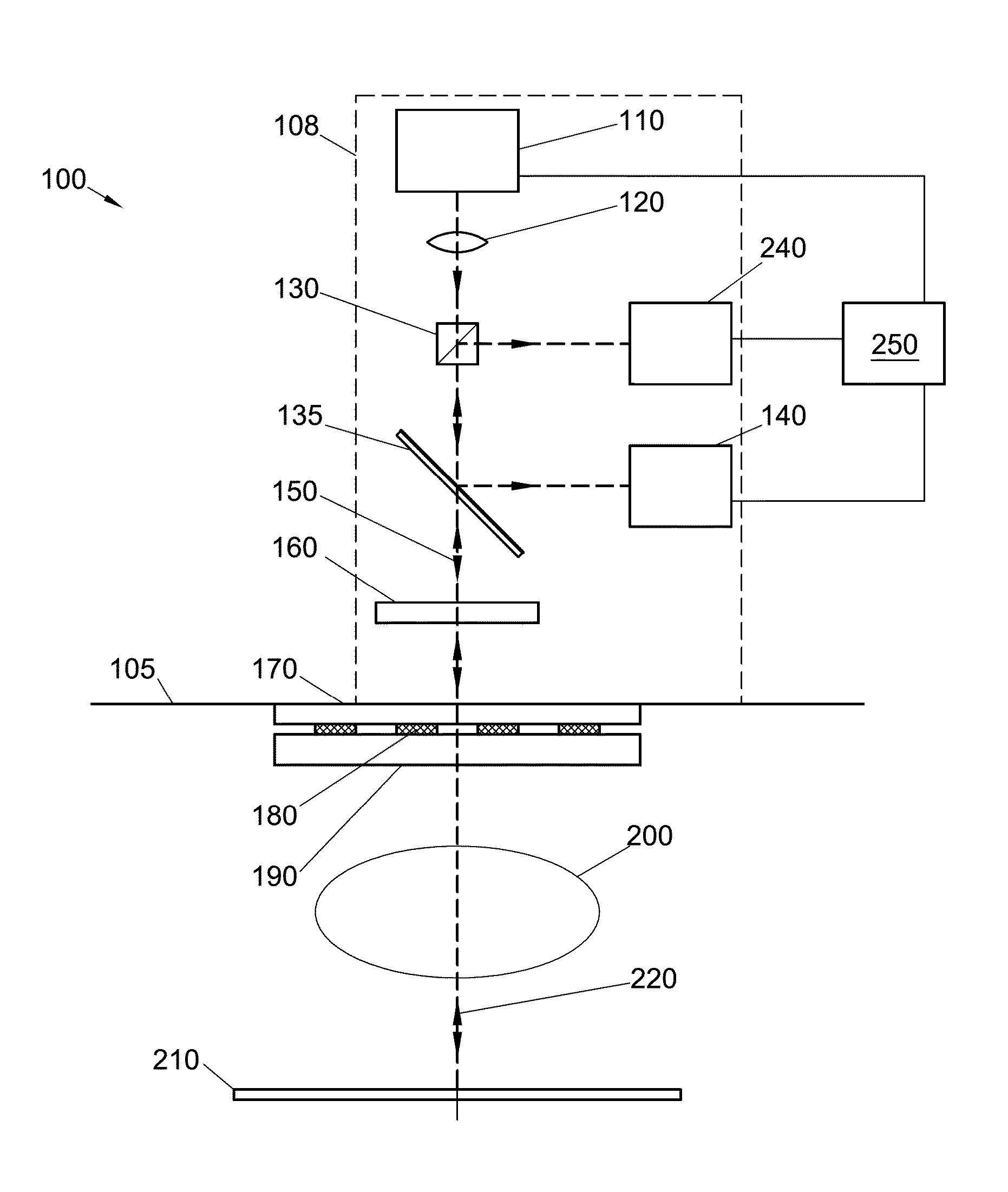
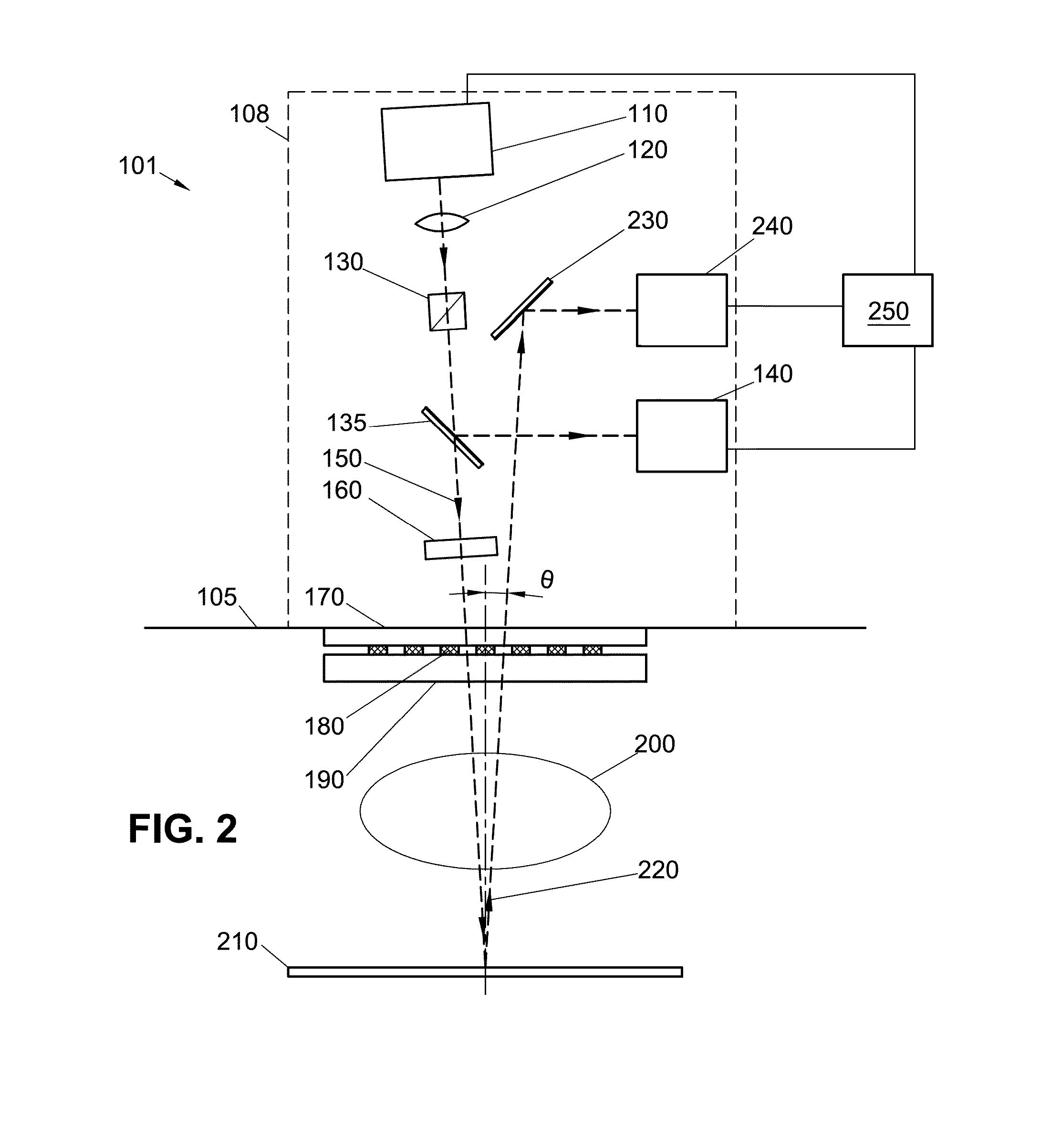
[0023]In the following description, in order to facilitate a thorough understanding of the invention and for purposes of explanation and not limitation, specific details are set forth, such as particular geometries of a lithography, coater / developer, and gap-fill treatment system, and descriptions of various components and processes. However, it should be understood that the invention may be practiced in other embodiments that depart from these specific details.

[0024]In the description to follow, the terms radiation-sensitive material and photoresist may be used interchangeably, photoresist being only one of many suitable radiation-sensitive materials for use in photolithography. Similarly, hereinafter the term substrate, which represents the workpiece being processed, may be used interchangeably with terms such as semiconductor wafer, LCD panel, light-emitting diode (LED), photovoltaic (PV) device panel, etc., the processing of all of which falls within the scope of the claimed inv...


PUM

PropertyMeasurementUnit
Angleaaaaaaaaaa
Angleaaaaaaaaaa
Thicknessaaaaaaaaaa

Abstract

Disclosed is an in-situ optical monitor (ISOM) system and associated method for controlling plasma etching processes during the forming of stepped structures in semiconductor manufacturing. The in-situ optical monitor (ISOM) can be optionally configured for coupling to a surface-wave plasma source (SWP), for example a radial line slotted antenna (RLSA) plasma source. A method is described to correlate the lateral recess of the steps and the etched thickness of a photoresist layer for use with the in-situ optical monitor (ISOM) during control of plasma etching processes in the forming of stepped structures.

Description

CROSS REFERENCE TO RELATED APPLICATIONS[0001]This application is based on and claims the benefit of and priority to co-pending U.S. Provisional Patent Application No. 61 / 672,880, entitled “SYSTEM FOR IN-SITU FILM STACK MEASUREMENT DURING ETCHING AND ETCH CONTROL METHOD” (Ref. No. TTI-239PROV), filed on Jul. 18, 2012, the entire contents of which are herein incorporated by reference.BACKGROUND OF THE INVENTION[0002]1. Field of the Invention[0003]The present invention relates to a method and system for controlling the process of etching a structure on a substrate, for example, in semiconductor manufacturing. More particularly, it relates to a system and method for control of an etch process for forming of a structure with a feature, or multiple features in the horizontal direction, for example a stepped structure, on the substrate.[0004]2. Description of Related Art[0005]Plasma etch processes are commonly used in conjunction with photolithography in the process of manufacturing semico...

Claims


Application Information

Patent Timeline
IPC IPC(8): H01L21/66
CPCH01L22/12H01J37/32972H01L22/26
Inventor LI, SHIFANGBAO, JUNWEICHU, HANYOUJIN, WENMENG, CHING-LINGXU, WEIWENWANG, PINGTUITJE, HOLGERMIHAYLOV, MIHAILTIAN, XINKANG
Owner TOKYO ELECTRON LTD
Why Eureka
Try Eureka