Method and apparatus to fold optics in tools for measuring shape and/or thickness of a large and thin substrate

a technology of optics and folding optics, which is applied in the direction of mirrors, instruments, measurement devices, etc., can solve the problems of measuring tools that cannot physically fit in a space, measuring tools are much more expensive, and the size of measuring tools is large, so as to achieve the effect of increasing length, reducing cost and increasing the size of optical components

Active Publication Date: 2014-01-30
KLA TENCOR TECH CORP
View PDF4 Cites 0 Cited by
  • Summary
  • Abstract
  • Description
  • Claims
  • Application Information

AI Technical Summary

Benefits of technology

[0006]In one embodiment of the present invention, a measuring device includes mirrors for directing the optical path along an axis parallel to an axis normal to the surface of the wafer. Such configuration allows utilization of the space along the length of the measuring tool.
[0007]In another embodiment of the present invention, a method for measuring semiconductor wafers includes reflecting an interf...

Problems solved by technology

One disadvantage of this method is that the size of the measuring tool is large due to the size of imaging optics.
Simply scaling up existing measuring tools designed for a 300 mm wafer to accommodate a 450 mm ...

Method used


Image

  • Method and apparatus to fold optics in tools for measuring shape and/or thickness of a large and thin substrate
  • Method and apparatus to fold optics in tools for measuring shape and/or thickness of a large and thin substrate
  • Method and apparatus to fold optics in tools for measuring shape and/or thickness of a large and thin substrate

Examples


Embodiment Construction

[0013]Reference will now be made in detail to the subject matter disclosed, which is illustrated in the accompanying drawings. The scope of the invention is limited only by the claims; numerous alternatives, modifications and equivalents are encompassed. For the purpose of clarity, technical material that is known in the technical fields related to the embodiments has not been described in detail to avoid unnecessarily obscuring the description.

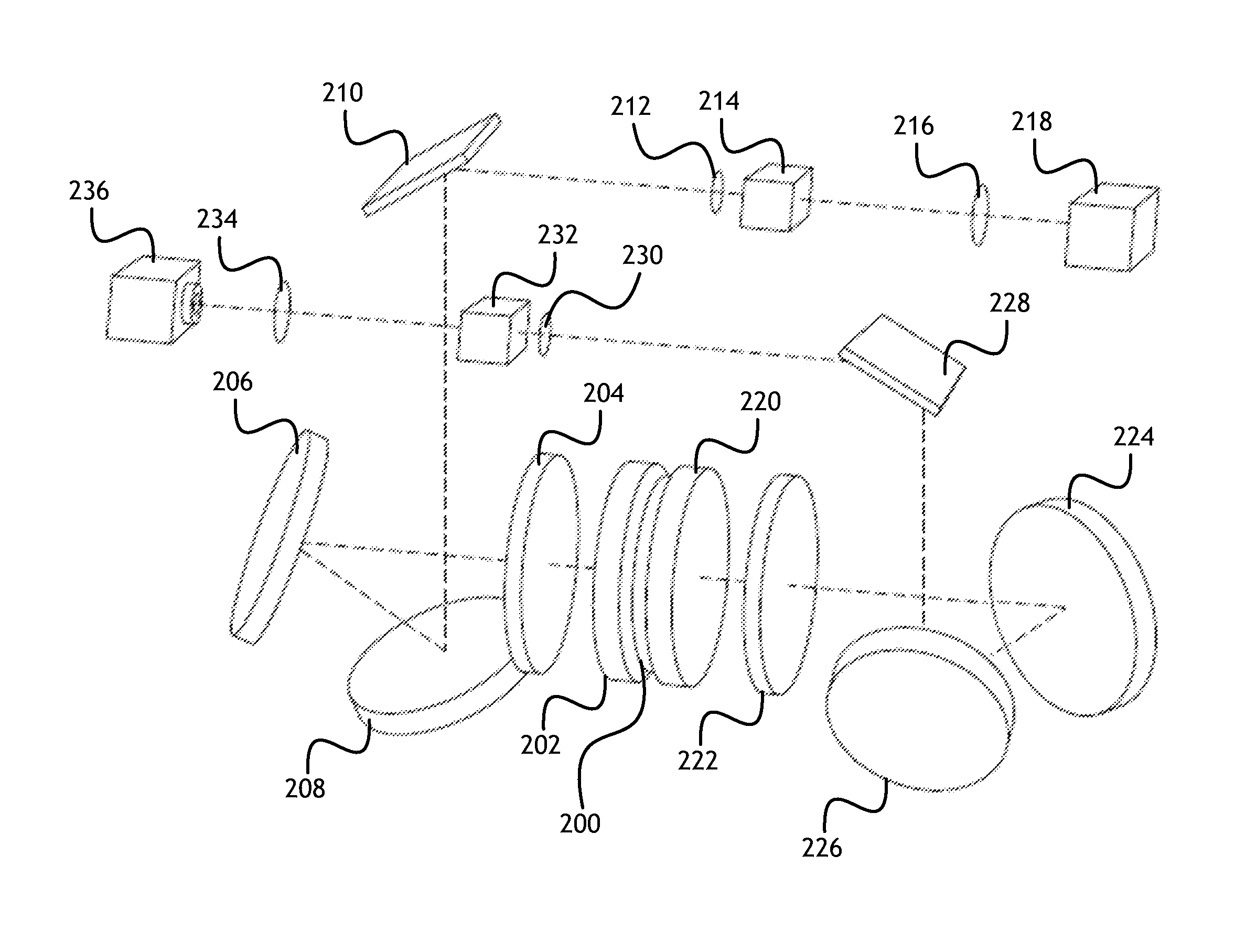
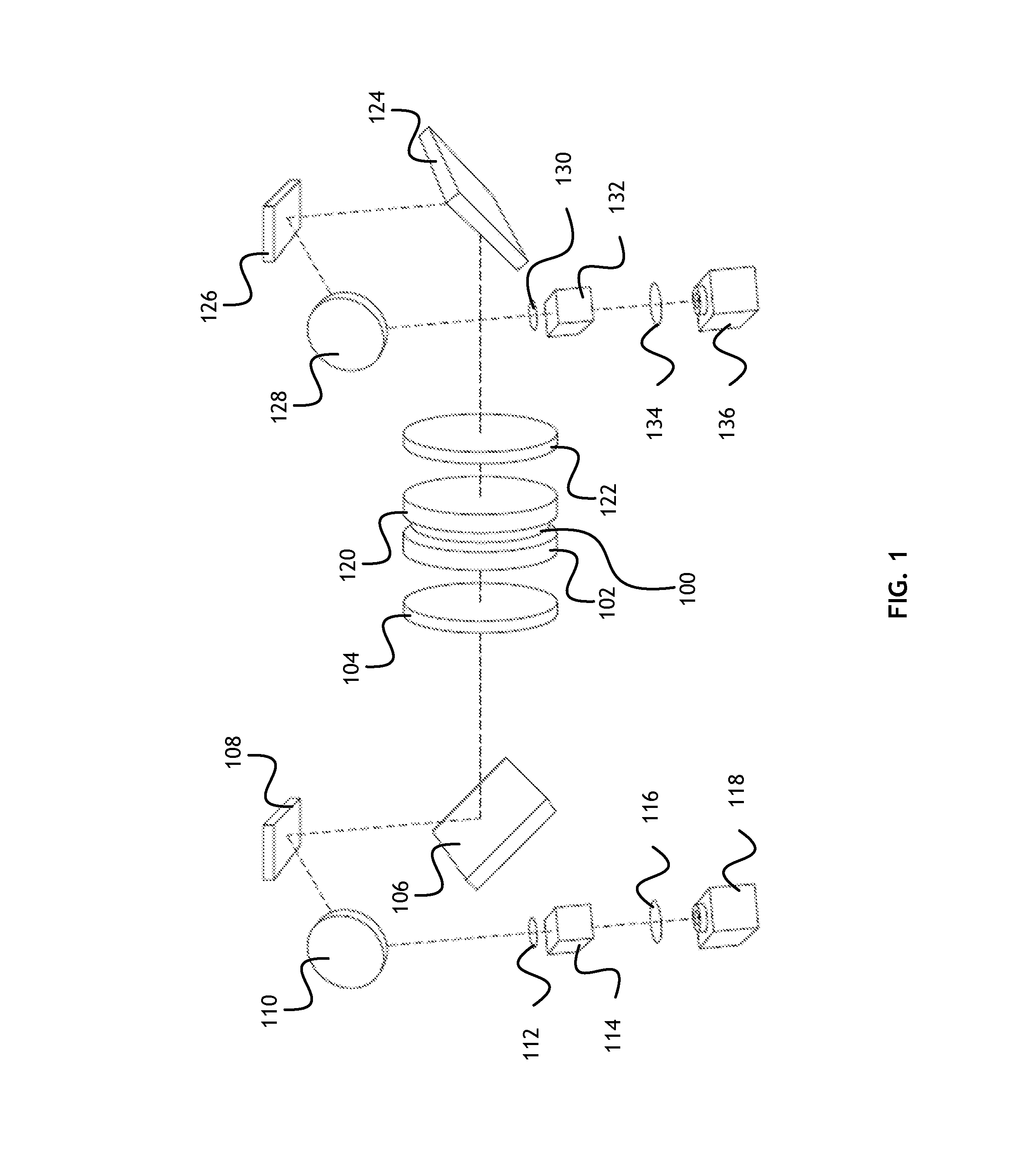
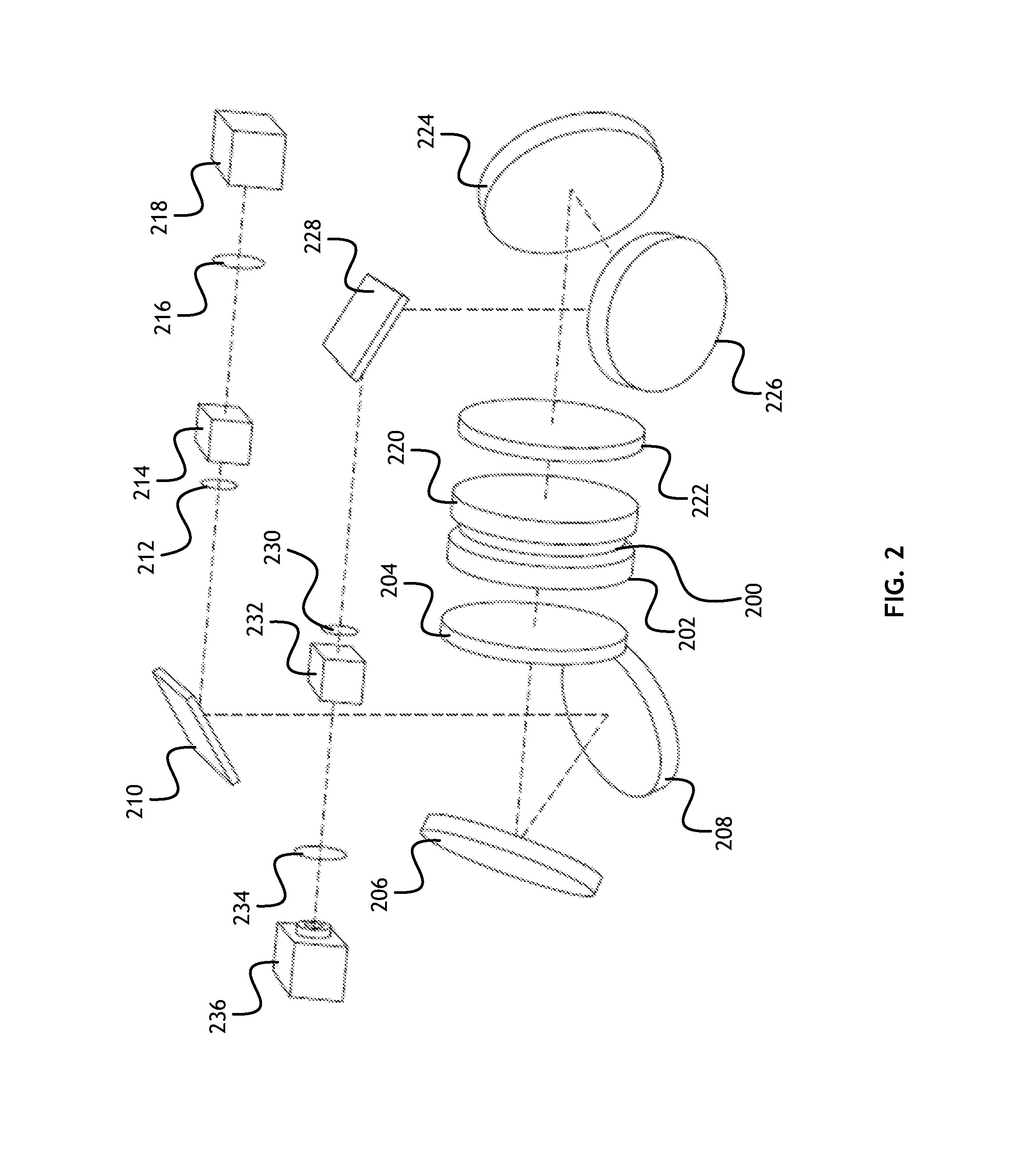
[0014]Referring to FIG. 1, a perspective view of a measuring tool is shown. The measuring tool may include one or two reference flats 102, 120. Reference flats 102, 120 are the references for measuring surface flatness of a semiconductor wafer 100. The measuring tool may also include one or two collimators 104, 122. Collimators 104, 122 narrow or collimate light from a semiconductor wafer 100. The measuring tool may also include one or more series of folding mirrors 106, 108, 110, 124, 126, 128.

[0015]Each series of folding mirrors 106, 108, 1...


PUM


Abstract

A semiconductor measuring tool has a folding mirror configuration that directs a light beam to pass the same space multiple times to reduce the size and footprint. Furthermore, the folding mirrors may reflect the light beam at less than forty-five degrees; thereby allowing for smaller folding mirrors as compared to the prior art.

Description

FIELD OF THE INVENTION[0001]The present invention is directed generally toward semiconductor wafer processing and more particularly toward measuring the shape and thickness of semiconductor wafers.BACKGROUND OF THE INVENTION[0002]In a typical tool for measuring the shape and thickness of a silicon wafer, two channels of interferometers are employed to measure both surfaces of the wafer. Each interferometer usually comprises lenses that image the wafer to a video camera. This way the whole wafer can be measured by the camera with millions of pixels, eliminating the need to mechanically scan the wafer, and the throughput is dramatically improved compared to scanning systems.[0003]One disadvantage of this method is that the size of the measuring tool is large due to the size of imaging optics. As the semiconductor industry shifts to larger wafers (for example from 300 mm to 450 mm) the size of the measuring tool may increase significantly. Simply scaling up existing measuring tools des...

Claims


Application Information

Patent Timeline
IPC IPC(8): G01B11/06G02B5/08
CPCG01B9/0203G01B9/02021G01B11/2441G01B2290/70G01B11/06H04N23/00G01B11/24G02B17/008G02B27/283
Inventor WANG, CHUNHAIHUANG, CHUNSHENGZENG, ANDREW ANGOODMAN, FREDERICK ARNOLDTANG, SHOUHONGZHANG, YI
Owner KLA TENCOR TECH CORP
Why Eureka
Try Eureka