Oxide semiconductor stacked film and semiconductor device

a technology of stacked film and semiconductor devices, which is applied in semiconductor devices, semiconductor/solid-state device testing/measurement, electrical apparatus, etc., can solve the problems of reducing the reliability of a semiconductor device including the transistor, and achieve the effect of not easily causing a variation in the electrical characteristics of a transistor, stable electrical characteristics, and high stability

Active Publication Date: 2014-02-06
SEMICON ENERGY LAB CO LTD
View PDF1 Cites 52 Cited by
  • Summary
  • Abstract
  • Description
  • Claims
  • Application Information

AI Technical Summary

Benefits of technology

[0017]With one embodiment of the present invention, an oxide semiconductor stacked film which does not easily cause a variation in electrical characteristics of a transistor and has high stability can be provided. Further, a transistor

Problems solved by technology

A transistor using an oxide semiconductor has a problem in that the electrical characteristics, typically, the threshold voltages, are varied with time or through the gate bias

Method used


Image

  • Oxide semiconductor stacked film and semiconductor device
  • Oxide semiconductor stacked film and semiconductor device
  • Oxide semiconductor stacked film and semiconductor device

Examples


embodiment 1

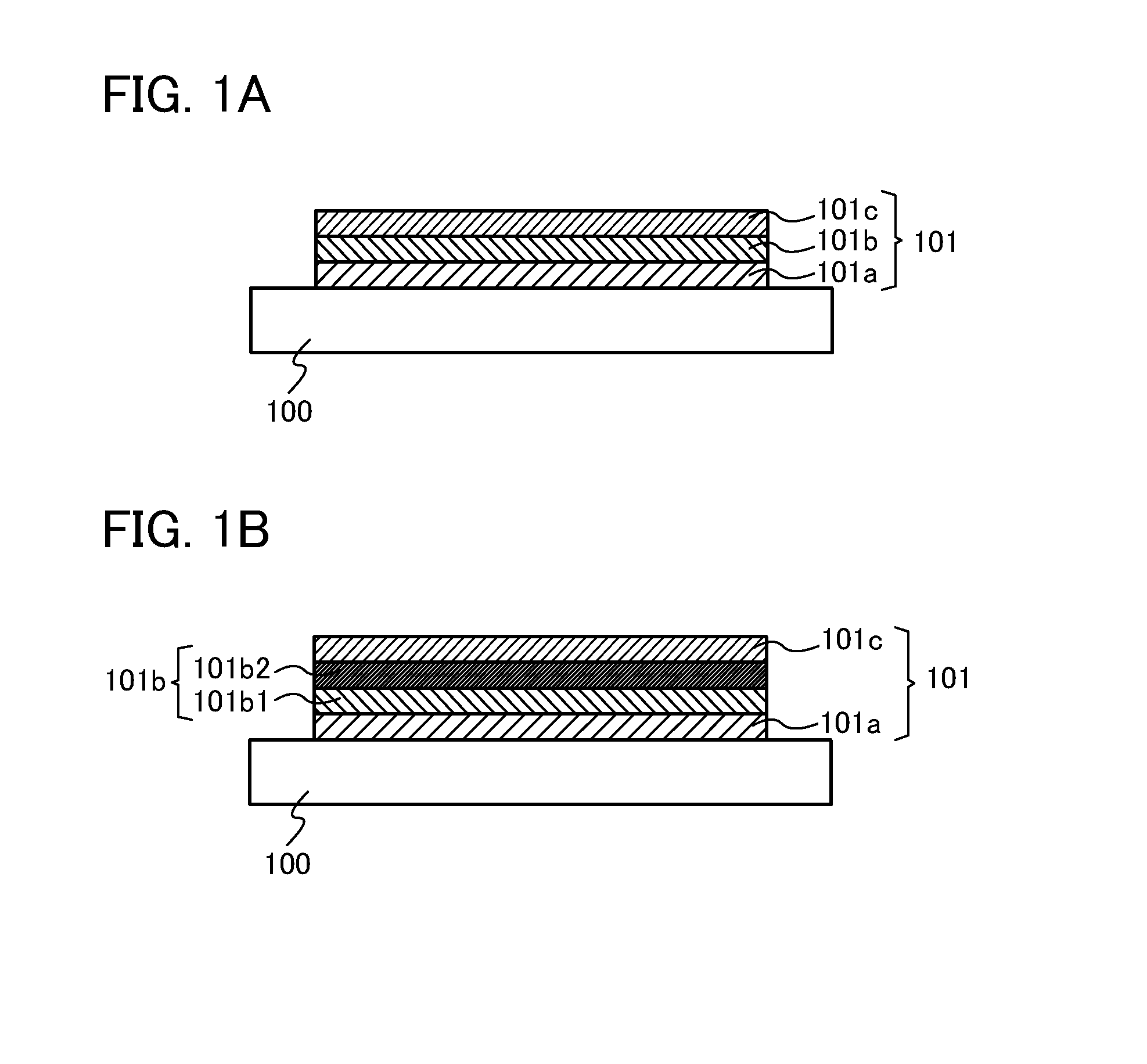
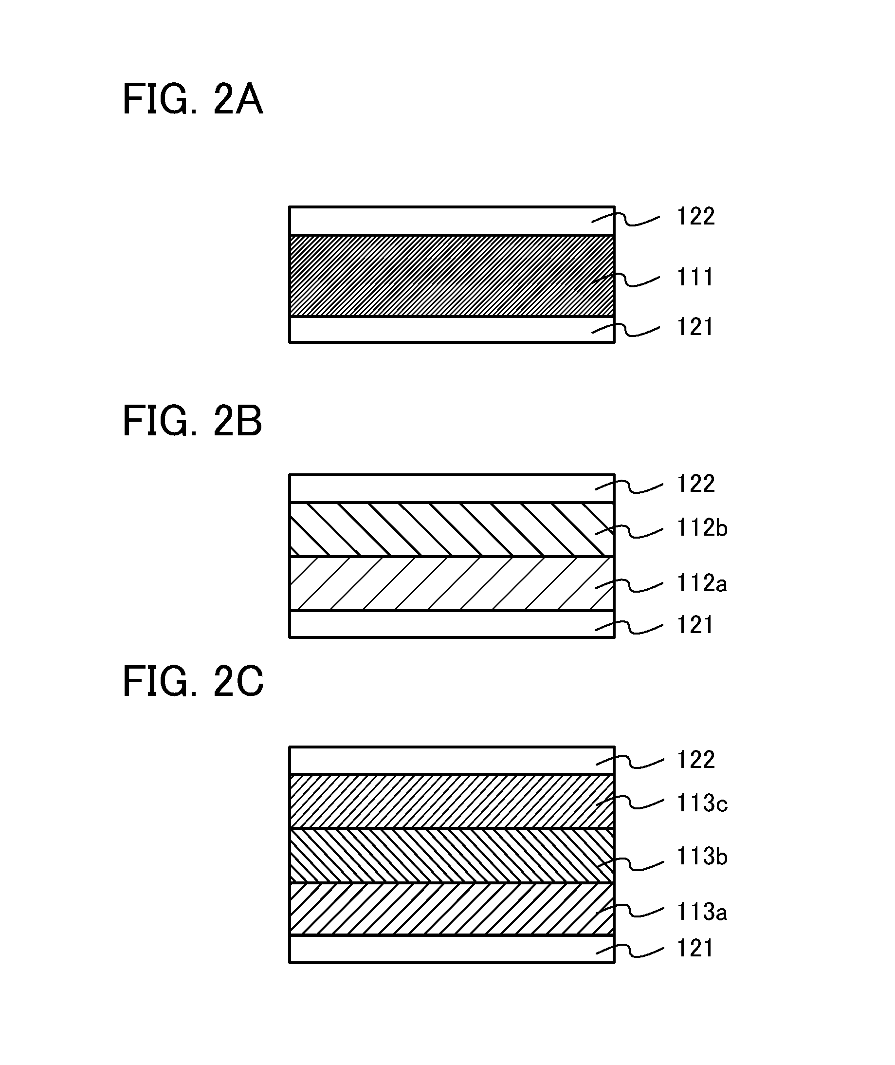
[0039]In this embodiment, an oxide semiconductor stacked film of one embodiment of the present invention is described with reference to FIGS. 1A and 1B.

[0040]FIG. 1A illustrates an oxide semiconductor stacked film 101 provided over a substrate 100. The oxide semiconductor stacked film 101 includes a plurality of oxide semiconductor layers, and for example, a first oxide semiconductor layer 101a, a second oxide semiconductor layer 101b, and a third oxide semiconductor layer 101c are sequentially stacked in the oxide semiconductor stacked film 101.

[0041]The oxide semiconductor layers 101a to 101c each include indium, gallium, and zinc at different atomic ratios. Among the oxide semiconductor layers 101a to 101c, for example, the content percentage of indium in the second oxide semiconductor layer 101b is preferably higher than that in the first oxide semiconductor layer 101a and is preferably higher than that in the third oxide semiconductor layer 101c.

[0042]Furthermore, in the secon...

embodiment 2

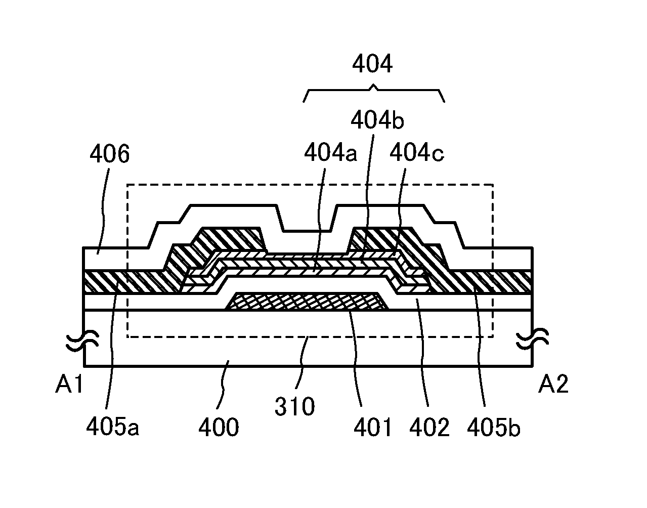
[0103]In this embodiment, embodiments of semiconductor devices of one embodiment of the present invention are described with reference to FIGS. 4A to 4C, FIGS. 5A and 5B, FIGS. 6A and 6B, and FIGS. 7A and 7B.

[0104]There is no particular limitation on the structure of the transistor included in a semiconductor device of one embodiment of the present invention; for example, a staggered type or a planar type having a top-gate structure or a bottom-gate structure can be employed. Further, the transistor may have a single-gate structure including one channel formation region, or a multi-gate structure such as a double-gate structure including two channel formation regions or a triple-gate structure including three channel formation regions. Alternatively, the transistor may have a dual-gate structure including two gate electrode layers positioned above and below a channel formation region with a gate insulating film provided therebetween.

[0105]FIGS. 4A to 4C illustrate a structural examp...

embodiment 3

[0140]In this embodiment, a method for manufacturing the transistor using the oxide semiconductor stacked film illustrated in FIGS. 4A to 4C is described with reference to FIGS. 8A to 8E.

[0141]First, the gate electrode layer 401 is formed over the substrate 400 (see FIG. 8A).

[0142]There is no particular limitation on a substrate that can be used as the substrate 400 having an insulating surface as long as it has heat resistance enough to withstand heat treatment performed later. A variety of glass substrates for electronics industry, such as a barium borosilicate glass substrate and an aluminoborosilicate glass substrate, can be used as the substrate 400. Note that as the substrate, a substrate having a thermal expansion coefficient of greater than or equal to 25×10−7 / ° C. and less than or equal to 50×10−7 / ° C. (preferably greater than or equal to 30×10−7 / ° C. and less than or equal to 40×10−7 / ° C.) and a strain point of higher than or equal to 650° C. and lower than or equal to 750...


PUM


Abstract

An oxide semiconductor stacked film which does not easily cause a variation in electrical characteristics of a transistor and has high stability is provided. Further, a transistor which includes the oxide semiconductor stacked film in its channel formation region and has stable electrical characteristics is provided. An oxide semiconductor stacked film includes a first oxide semiconductor layer, a second oxide semiconductor layer, and a third oxide semiconductor layer which are sequentially stacked and each of which contains indium, gallium, and zinc. The content percentage of indium in the second oxide semiconductor layer is higher than that in the first oxide semiconductor layer and the third oxide semiconductor layer, and the absorption coefficient of the oxide semiconductor stacked film, which is measured by the CPM, is lower than or equal to 3×10⁻³/cm in an energy range of 1.5 eV to 2.3 eV.

Description

TECHNICAL FIELD[0001]The present invention relates to a method for manufacturing a semiconductor device including an oxide semiconductor stacked film and a field-effect transistor.BACKGROUND ART[0002]Transistors used for most flat panel displays typified by a liquid crystal display device and a light-emitting display device are formed using silicon semiconductors such as amorphous silicon, single crystal silicon, and polycrystalline silicon provided over glass substrates. Further, transistors formed using such silicon semiconductors are used in integrated circuits (ICs) and the like.[0003]In recent years, attention has been drawn to a technique in which, instead of a silicon semiconductor, a metal oxide exhibiting semiconductor characteristics is used for transistors. Note that in this specification and the like, a metal oxide exhibiting semiconductor characteristics is referred to as an oxide semiconductor.[0004]For example, a technique is disclosed in which a transistor is manufac...

Claims


Application Information

Patent Timeline
IPC IPC(8): H01L29/24H01L29/786
CPCH01L29/78693H01L29/247H01L29/78696H01L22/14H01L2924/0002H01L29/78606H01L29/1054H01L29/42384H01L29/7869H01L2924/00H01L2924/13069H01L29/42356
Inventor YAMAZAKI, SHUNPEITSUBUKU, MASASHIWATANABE, RYOSUKEOOTA, MASASHIISHIHARA, NORITAKAINOUE, KOKI
Owner SEMICON ENERGY LAB CO LTD
Why Eureka
Try Eureka