

Boron nitride antistiction films and methods for forming same
a technology of boron nitride and anti-static coating, which is applied in the direction of static indicating devices, instruments, optical elements, etc., can solve problems such as surface wear, and achieve the effect of reducing stiction and reducing stiction
- Summary
- Abstract
- Description
- Claims
- Application Information
AI Technical Summary
Benefits of technology
Problems solved by technology
Method used
Image

Examples
Embodiment Construction
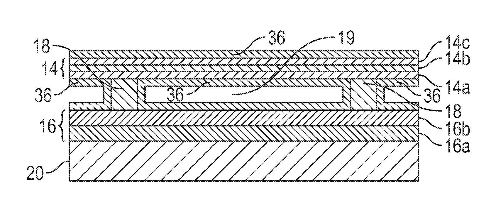
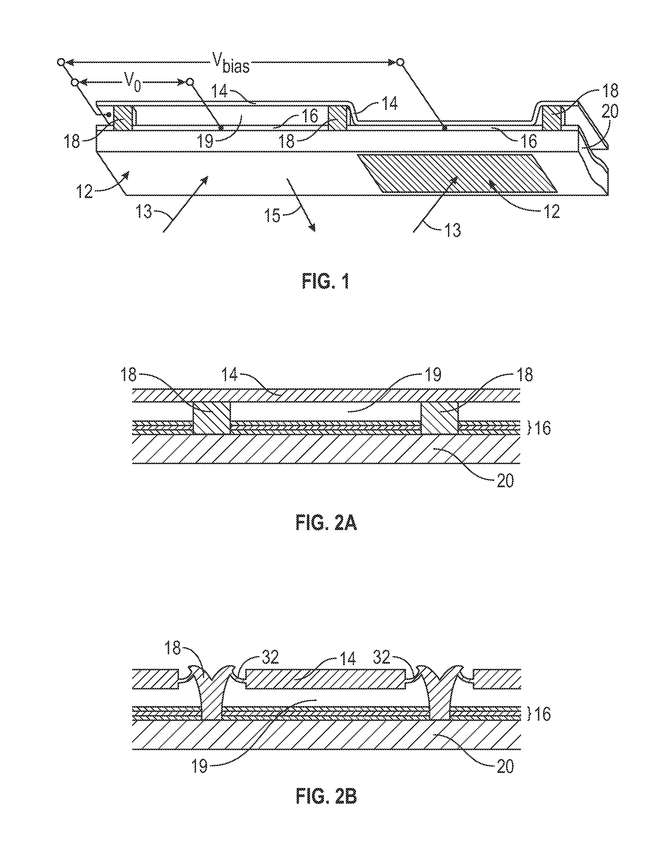
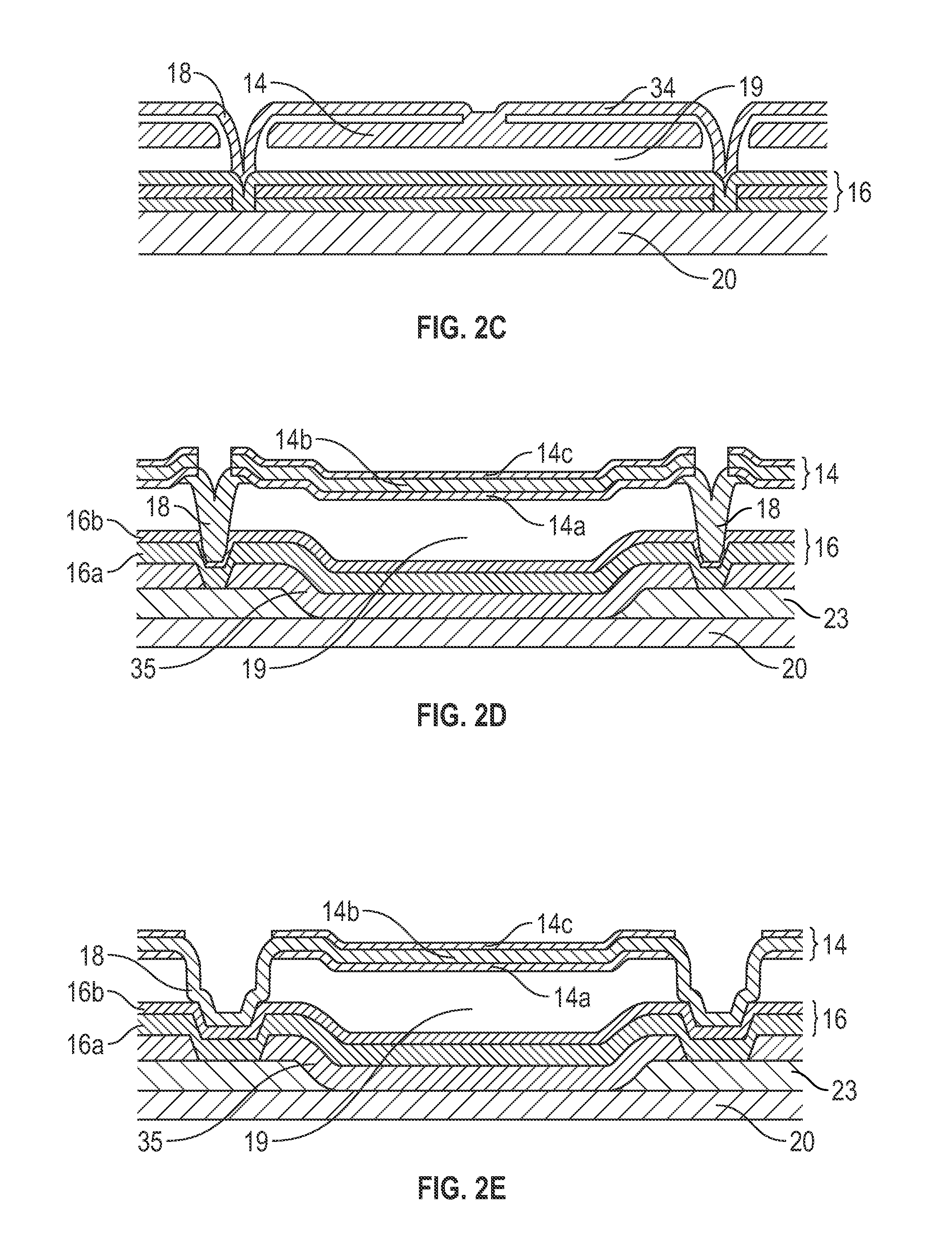
[0026]The following description is directed to certain implementations for the purposes of describing the innovative aspects of this disclosure. However, a person having ordinary skill in the art will readily recognize that the teachings herein can be applied in a multitude of different ways. The described implementations may be implemented in any device, apparatus, or system that can be configured to display an image, whether in motion (such as video) or stationary (such as still images), and whether textual, graphical or pictorial. More particularly, it is contemplated that the described implementations may be included in or associated with a variety of electronic devices such as, but not limited to: mobile telephones, multimedia Internet enabled cellular telephones, mobile television receivers, wireless devices, smartphones, Bluetooth® devices, personal data assistants (PDAs), wireless electronic mail receivers, hand-held or portable computers, netbooks, notebooks, smartbooks, ta...
PUM
| Property | Measurement | Unit |
|---|---|---|
| thickness | aaaaa | aaaaa |
| thickness | aaaaa | aaaaa |
| thickness | aaaaa | aaaaa |
Abstract
Description
Claims
Application Information