Liquid crystal display device and method for driving the same

a liquid crystal display and display device technology, applied in the direction of electric digital data processing, instruments, computing, etc., can solve the problems of increasing power consumption, increasing the power consumption, and the amount of change in data signal voltage, so as to reduce the power consumption of the liquid crystal display device

Active Publication Date: 2014-02-13
SEMICON ENERGY LAB CO LTD
View PDF3 Cites 18 Cited by
  • Summary
  • Abstract
  • Description
  • Claims
  • Application Information

AI Technical Summary

Benefits of technology

[0009]High display quality is required for liquid crystal display devices, and driving frequencies of liquid crystal display devices tend to be increased (e.g., to 120 Hz or 240 30 Hz, an integral multiple of 60 Hz) along with an increase in the number of pixels for higher definition and higher resolution. Therefore, techniques for reducing power consumption due to the increase in driving frequencies have been demanded.
[0012]In view of the above, an object of one embodiment of the present invention is to provide a liquid crystal display device which consumes less power and a method for driving the liquid crystal display device.
[0016]According to the present invention, power consumption of a liquid crystal display device can be reduced.

Problems solved by technology

However, in inversion driving in which the polarity of a data signal written into a pixel is changed every frame period, the amount of change in data signal voltage due to rewriting of a pixel is large even when the strength of an electric field which acts upon liquid crystal is unchanged; this leads to an increase in power consumption.
This problem becomes more prominent with an increase in driving frequency or an increase in screen size.

Method used


Image

  • Liquid crystal display device and method for driving the same
  • Liquid crystal display device and method for driving the same
  • Liquid crystal display device and method for driving the same

Examples


embodiment 1

[0030]Examples of a liquid crystal display device and a method for driving the liquid crystal display device are described with reference to FIG. 1, FIG. 2, FIG. 3, FIG. 4, FIG. 5, FIG. 6, FIG. 7, and FIGS. 8A and 8B.

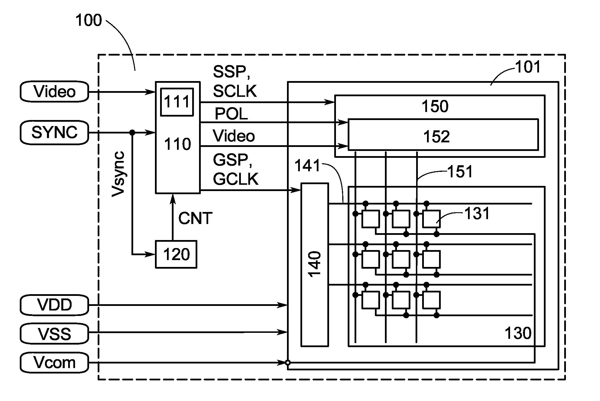
[0031]FIG. 1 is a block diagram illustrating a structural example of a liquid crystal display device in this embodiment. As shown in FIG. 1, a liquid crystal display device 100 includes a liquid crystal panel 101, a control circuit 110, and a counter circuit 120.

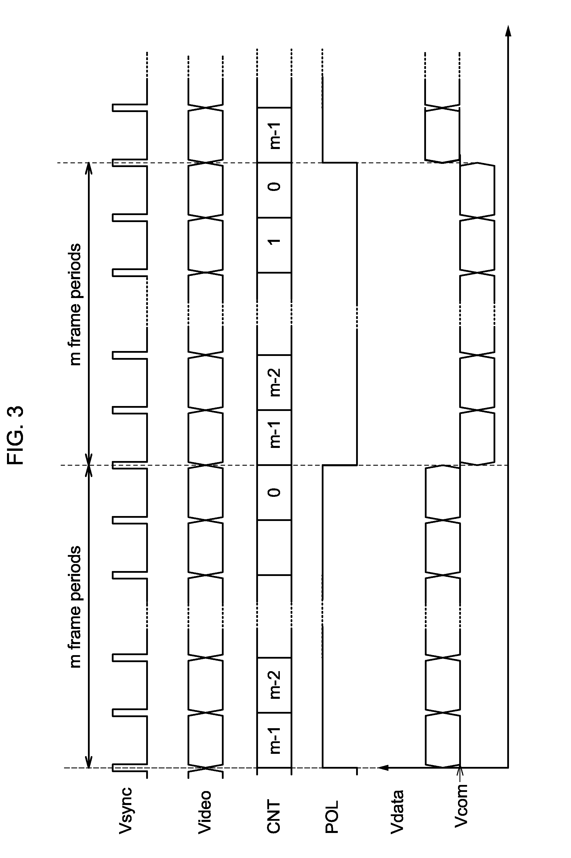
[0032]An image signal (Video), which is digital data, and a synchronization signal (SYNC) for controlling rewriting of a screen of the liquid crystal panel 101 are input to the liquid crystal display device 100. Examples of a synchronization signal include a horizontal synchronization signal (Hsync), a vertical synchronization signal (Vsync), and a reference clock signal (CLK).

[0033]The liquid crystal panel 101 includes a display portion 130, a scan line driver circuit 140, and a data line driver circuit 150. Th...

embodiment 2

[0092]In this embodiment, a structure of the liquid crystal panel 101 is described with reference to FIGS. 9A to 9C.

[0093]FIGS. 9A and 9B are plan views of the liquid crystal panel 101. FIG. 9C is a cross-sectional view showing a structural example of the liquid crystal panel 101, and corresponds to a cross section along line M-N in FIGS. 9A and 9B.

[0094]The liquid crystal panel 101 has a structure in which a liquid crystal layer 4008 is sealed between a substrate 4001 and a substrate 4006 with a sealant 4005.

[0095]A light-transmitting substrate can be used as each of the substrates 4001 and 4006. For example, a substrate made of glass, ceramics, plastics, or the like can be used. Examples of plastic substrates include a fiberglass-reinforced plastics (FRP) substrate, a polyvinyl fluoride (PVF) film, a polyester film, and an acrylic resin film.

[0096]A display portion 4002 including a plurality of pixels and a scan line driver circuit 4004 are provided in a region surrounded by the s...

embodiment 3

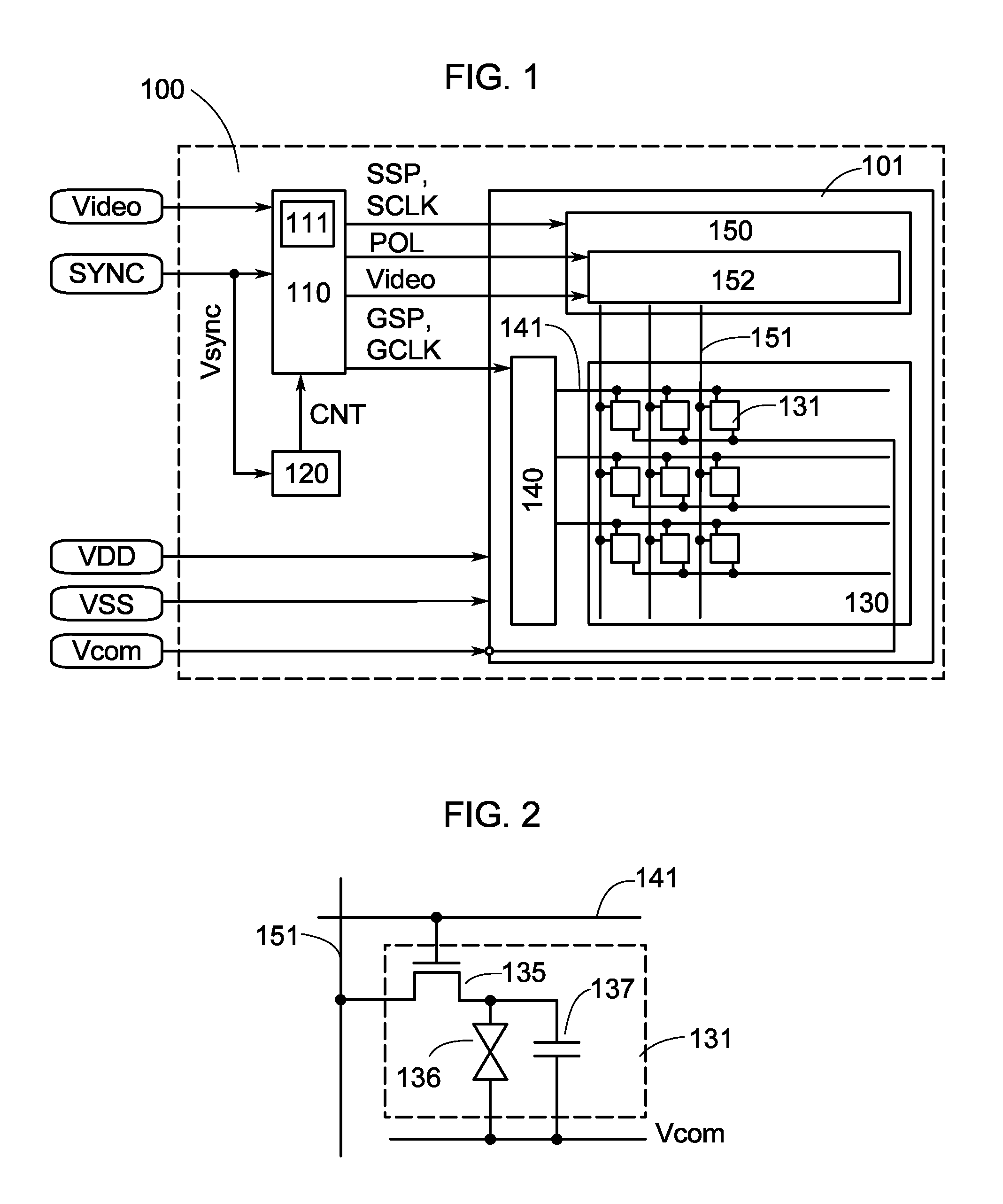
[0139]In this embodiment, a structure of the liquid crystal element 136 in FIG. 2 is described. As mentioned in Embodiment 2, the structure of the liquid crystal element differs depending on the display mode of a liquid crystal display device.

[0140]FIGS. 10A to 10D are cross-sectional views showing structural examples of liquid crystal elements in respective display modes. FIG. 10A shows a twisted nematic (TN) mode or a vertical alignment (VA) mode, FIG. 10B shows a multi-domain vertical alignment (MVA) mode, FIG. 10C shows an in-plane-switching (IPS) mode, and FIG. 10D shows a fringe field switching (FFS) mode.

[0141]As shown in FIGS. 10A to 10D, the liquid crystal element includes a pixel electrode 5001, a common electrode 5002, and a liquid crystal layer 5003. The liquid crystal layer 5003 is provided between a substrate 5011 and a substrate 5012.

[0142]As shown in FIG. 10A, the liquid crystal element has the same structure in the TN mode and the VA mode. In the VA mode liquid crys...


PUM


Abstract

Power consumed in a liquid crystal display device owing to inversion driving is reduced. A control circuit generates a polarity control signal whose potential level is switched at intervals of two or more frame periods. A data line driver circuit processes an image signal to generate a data signal. The data signal has a polarity corresponding to the potential level of the polarity control signal. The control circuit stops output of the image signal to the data line driver circuit when determining that there is no motion in data of the image signal. The control circuit controls a scan line driver circuit and the data line driver circuit, thereby performing, in response to a change in the potential level of the polarity control signal, rewriting of a display portion at least in one frame period during a period in which the output of the image signal is stopped.

Description

BACKGROUND OF THE INVENTION[0001]1. Field of the Invention[0002]The present invention relates to a liquid crystal display device and a method for driving the liquid crystal display device.[0003]2. Description of the Related Art[0004]In view of fossil fuel exhaustion, environmental problems, and the like, all kinds of electronic devices are required to consume less power. Liquid crystal display devices are no exception. For example, techniques of reducing the frequency of rewriting pixels in order to reduce power consumption of a liquid crystal display device have been reported (see the following references).REFERENCES Patent Documents [0005][Patent Document 1] United States Patent No. 7321353[0006][Patent Document 2] Japanese Published Patent Application No. 2011-145667[0007][Non-Patent Document][0008][Non-Patent Document 1] K. Tsuda et al., IDW'02, Proc., pp. 295-298SUMMARY OF THE INVENTION[0009]High display quality is required for liquid crystal display devices, and driving freque...

Claims


Application Information

Patent Timeline
Patent Type & Authority Applications(United States)
IPC IPC(8): G09G3/36
CPCG09G3/3696G09G3/3614G09G3/3648G09G2310/065G09G2310/08G09G2330/02G02F1/133G09G3/36
Inventor YAMAZAKI, SHUNPEIKOYAMA, JUNHIRAKATA, YOSHIHARUMIYAKE, HIROYUKI
Owner SEMICON ENERGY LAB CO LTD
Why Eureka
Try Eureka